NovaSilicon Paper: Chipmaking Bottleneck Isn't Tools, It's Organization

NovaSilicon has closed two consecutive rounds of financing totaling nearly 100 million RMB within three months of its founding, and has already signed multi-million-RMB orders with top-tier industry customers.
RSI (Recursive Self-Improvement) is becoming one of the most closely watched frontiers in artificial intelligence.
When models can autonomously generate tasks, automatically verify results, and convert every trial-and-error cycle into accumulated capability, intelligence growth breaks free from its dependence on human data for the first time, entering a trajectory of self-compounding returns.
As AI enters the era of self-evolution, the entire industry is waiting for one answer: in which scenarios will RSI methodology land first.
Chip design has long been regarded as one of the most complex engineering tasks in the modern industrial system.
From transistor-level analog circuit design to digital logic synthesis, physical implementation, layout optimization, and final tape-out verification, the birth of an advanced chip spans dozens of specialized stages, involving semiconductor physics, circuit theory, computer architecture, algorithm optimization, and manufacturing processes, among other fields.
Yet it is precisely because of its unique deterministic verification system — DRC, LVS, and timing signoff serve as the "graders" — that chip design is becoming the track where RSI will first deliver commercial value and achieve industrial deployment.
NovaSilicon is a standout startup team riding this wave.
We recently learned that NovaSilicon announced the completion of a new funding round, led by SenseTime Guoxiang.
Founded in May 2026, the company has rapidly completed two consecutive rounds of financing totaling nearly RMB 100 million within just over a month, led by 5Y Capital and SenseTime Guoxiang respectively. The proceeds will be used primarily to continue building a super-intelligence system for the chip industry.
Going forward, NovaSilicon will advance along this technical roadmap, gradually constructing a super-intelligence system with complete chip engineer capabilities, covering every key stage of chip design.
The company's ultimate goal is to enable super-intelligence to directly execute real chip orders, from design and optimization to verification and delivery, achieving an intelligent upgrade of the entire chip design industry chain.
NovaSilicon's founder, Dr. Linyang Li, graduated from the School of Information Science and Technology at Fudan University for his undergraduate studies, and earned his PhD from Fudan University's Natural Language Processing Lab under Professor Xipeng Qiu. He is currently a Young Scientist at Shanghai Artificial Intelligence Laboratory and a postdoctoral researcher at The Chinese University of Hong Kong's Institute of Artificial Intelligence.
He participated in the development of MOSS, China's first open-source large language model, contributed to the pre-training and post-training of the Shusheng series of models, and led the team that completed InternThinker, China's first large model combining professional Go-playing capability with natural language explanatory reasoning.
Although it has been established for less than three months, NovaSilicon has already successfully developed several Super Intelligence Systems covering different stages of chip design, and signed multi-million-yuan orders with leading industry customers, which are about to be deployed at scale to significantly accelerate the speed and quality of chip delivery.
NovaSilicon recently published a methodological paper on the application of super-intelligence in the chip domain.
Paper: https://arxiv.org/abs/2608.14035
The paper provides a detailed analysis and introduction to the construction and operation of super-intelligence systems in the chip design process, including how to build a "Thinking Boundary Aware Super Intelligence," its fundamental differences from traditional AI EDA methods, and how this methodology can ultimately reshape the entire chip design industry and transform the industry chain.
This article is a detailed interpretation of that paper.

The Quest for Super-Intelligence in Chip Design
Over the past few decades, improvements in chip design efficiency have primarily relied on the development of EDA (Electronic Design Automation) tools.
EDA tools convert extensive manual design experience into software workflows, enabling engineers to complete complex design tasks with computer assistance. But as chip scales continue to grow and advanced processes evolve, traditional EDA methods are gradually approaching their own capability boundaries.
When an industry's complexity has exceeded what a single human brain, a single set of rules, or a single algorithm can bear, what form should AI take to intervene?
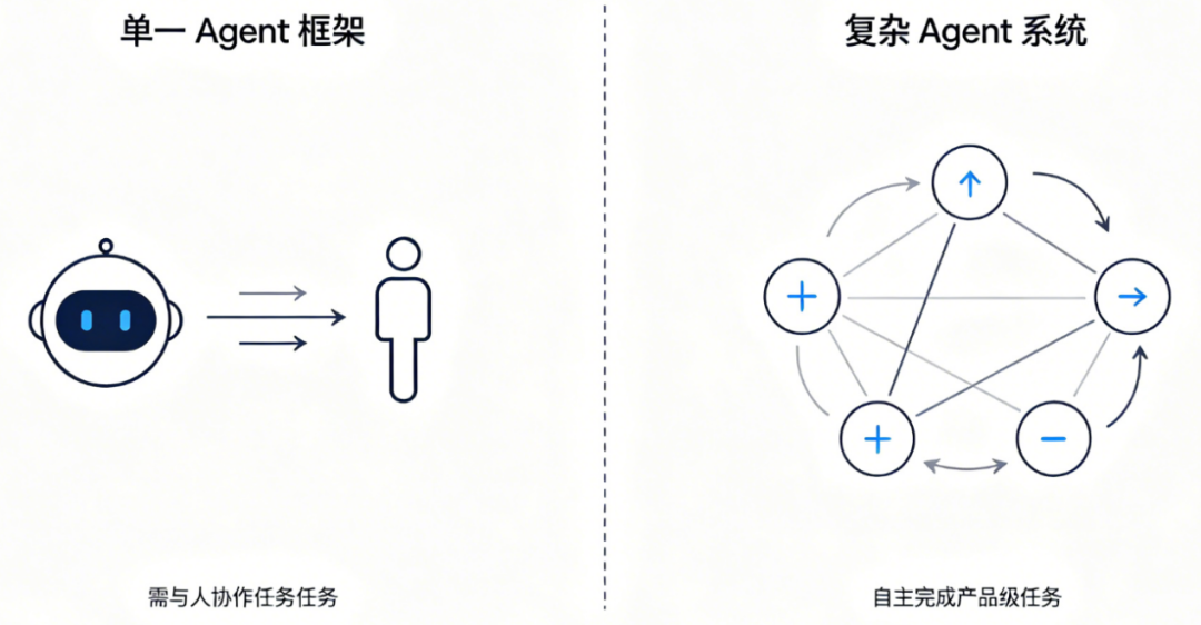
One possible answer is neither "a stronger optimizer" nor "a smarter Copilot," but rather an AI-organization —
Modeling chip design super-intelligence as an intelligent system composed of multiple agents capable of autonomous operation, autonomous collaboration, and autonomous evolution.
Behind this judgment lies a fundamental law of intelligentization for complex engineering systems.
The scale of problems a system can ultimately solve does not depend on how smart any single individual is, but on whether the system's organizational structure can bear sufficient complexity.

Why Does Chip Design Need a New AI Paradigm?
The essence of chip design is finding the optimal solution within an enormous design space that satisfies multiple constraints including performance, power, area, and reliability.
Take transistor sizing optimization in analog chip design as an example. An analog circuit typically contains numerous transistors, each with multiple key parameters, of which the most important are Width (W) and Length (L).
Different W/L combinations directly affect a transistor's drive capability, gain, bandwidth, noise, power consumption, and stability.
Thus, a seemingly simple sizing adjustment problem is fundamentally about finding the optimal solution in a high-dimensional continuous space.
Assuming a circuit contains 100 transistors, each requiring adjustment of W and L, the search space is theoretically a 200-dimensional or even higher-dimensional continuous space.
If process variations, temperature variations, voltage variations, matching constraints, and stability requirements are all factored in, the actual problem complexity increases further.
This is why traditional EDA typically relies heavily on human experience and mathematical optimization algorithms.

Human-Defined Search Spaces
Traditional EDA Methods and Bottlenecks
In traditional EDA flows, engineers typically do not let algorithms search the entire space directly.
The reason is simple: real-world design spaces are too vast for exhaustive search.
Therefore, engineers impose numerous rules in advance, such as Design Rules, Matching Constraints, Operating Region Constraints, Saturation Region restrictions, and various process experience rules.
These rules essentially help algorithms answer a critical question: which areas are worth searching, and which areas are meaningless.
In other words, human engineers use their knowledge and experience to perform manual pruning of the raw search space.
Afterward, algorithms employ methods such as Bayesian Optimization, genetic algorithms, and reinforcement learning to find optimal solutions within the reduced space.
This approach has been highly effective in the past because chip design knowledge was relatively stable, and human experts could summarize substantial experience.
But as chip complexity continues to increase, this model is beginning to hit bottlenecks.
The reason is that the growth rate of rules cannot keep pace with the growth rate of problem complexity.
In complex engineering, numerous failure cases are not caused by single factors, but often arise from combinations of multiple factors.
Factor A alone does not cause problems, factor B alone does not cause problems, and factor C presents no obvious risk either. But the combination of A+B+C+D may produce serious failures.
This "long-tail combination problem" is a typical characteristic of complex systems.
And combination spaces expand exponentially with dimensionality — human engineers cannot add rules indefinitely.
So the real problem is not "how to write more rules," but "who will define the search space in the future."

From Static Rules to Dynamic Cognition
AI Redefines Action Space
In artificial intelligence, Action Space determines what an agent can explore.
The upper limit of an intelligent system's capabilities depends largely on whether the problem space it faces is properly defined.
The traditional EDA path is: engineers define rules → algorithm searches → results obtained.
The future AI-driven chip design system may become: AI understands physical laws → dynamically judges valid space → autonomously searches → summarizes experience → updates strategy.
This is a shift from "static constraints" to "dynamic cognition."
The core change is not in the optimization algorithm itself, but in who possesses the ability to define the problem space.

LLM Enters Chip Design
From Data Fitting to Physical Understanding
The greatest limitation of traditional optimization algorithms is that they typically see only numbers.
For example, an optimizer might see [W1, L1, W2, L2, W3, L3...].
But it doesn't know which transistor W1 corresponds to, doesn't know what circuit structure that transistor sits in, doesn't know what physical mechanism parameter changes affect, and doesn't know which regions violate semiconductor physics.
It is essentially performing mathematical space search.
The value of large language models (LLMs) lies in their ability to introduce semantic understanding.
Applied to chip design, AI no longer sees just parameters, but the engineering meaning behind them.
For instance: why does a certain transistor need to enter the saturation region? Why does the gm/ID method guide analog design? Why is a certain topology suitable for low-power scenarios? Why are some parameter combinations mathematically feasible but physically unrealizable?
What LLMs provide is not simple predictive capability, but a "physical semantics engine."
Data is often sparse and task-specific; physical laws are universal and transferable.
This is precisely the important value of AI applied to scientific and engineering domains.

From Copilot to AI Organization
Currently, most AI+chip solutions on the market remain essentially assistive tools.
Examples include automatic code generation, automatic interpretation of simulation results, assisting engineers with debugging, and providing design suggestions.
These tools improve individual engineer efficiency.
But if the goal is to achieve paradigm change in chip design, merely improving individual efficiency is insufficient.
The reason is that the biggest constraint in the chip industry is no longer inadequate tools, but limited human cognitive bandwidth.
A complex chip project requires analog design experts, digital design experts, process experts, verification experts, physical implementation experts, system architecture experts, and more.
There is substantial complex collaboration between these roles.
Therefore, what is needed in the future is not just an AI engineer assistant, but an entire AI engineering organization.
Different agents assume different responsibilities: an architecture agent handles system planning, an analog design agent handles circuit optimization, a verification agent identifies problems, a process agent manages manufacturing constraints, an optimization agent explores the design space, and an evaluation agent makes trade-offs.
These agents continuously communicate, compete, verify, and learn from each other.
This is analogous to the evolution of modern software engineering from monolithic programs to microservices architecture: when system complexity exceeds what a single module can bear, scaling must be achieved through organization.
Taking AI-involved layout design tasks as an example, comparing heuristic rules, agent workflow methods, and fully autonomous agent system methods completing the same layout task reveals the progression of layout design capability.
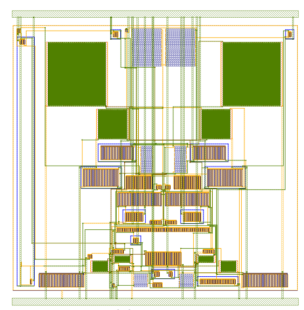
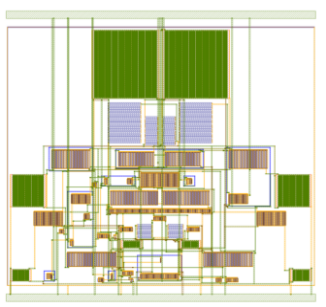
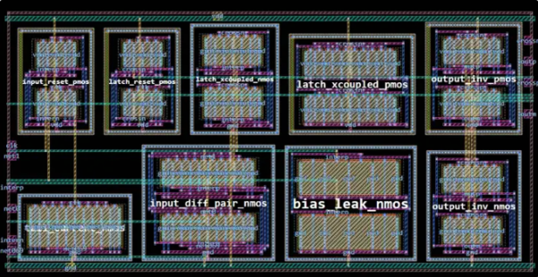
Figures (1), (2), and (3) show heuristic rules, agent workflow methods, and fully autonomous agent system methods respectively. (Image sources: https://arxiv.org/pdf/2608.13767; https://arxiv.org/abs/2608.14035)
Why now?
This AI-system-based approach can succeed primarily based on three changes.
First, LLM capabilities have crossed a critical threshold.
Past large models were mainly regarded as text generation tools.
But in recent years, LLMs have demonstrated long-chain reasoning capabilities, engineering knowledge understanding capabilities, cross-domain knowledge transfer capabilities, and tool-use capabilities.
They are evolving from "language models" toward "general reasoning systems."
Second, multi-agent systems are becoming a new form of AI organization.
From software development to scientific research automation, multi-agent systems are proving one thing: complex tasks do not necessarily require a super-model to complete, but can be accomplished through collaboration among multiple agents with different capabilities.
Chip design may become one of the most valuable application scenarios for this model.
Because chip design inherently features multi-disciplinary collaboration, long processes, high knowledge density, and high economic value.
Third, the chip industry needs a new speed scale.
Traditional chip design cycles are typically measured in months or even years.
If AI systems can truly assume design work, the design cycle for custom chips has the opportunity to shift from "based on human engineer work speed" to "based on AI system iteration speed."
This means chip innovation speed could change by orders of magnitude.
Future competition will be not just about who has more engineers, but about who possesses a continuously evolving chip design intelligence system.

From Program to Organization
A New Paradigm for Chip Design Intelligence
Traditional automation relies on fixed processes: step 1 → step 2 → step 3.
This approach suits problems with clear rules.
But truly complex problems require autonomous planning, dynamic decision-making, multi-agent collaboration, self-learning, and continuous optimization.
Therefore, the future direction for chip design AI is not simply automating EDA flows, but building intelligent organizations capable of autonomously completing engineering tasks.
Chip design super-intelligence is not a stronger software tool, but a new engineering production method.
In the future, gradually building a super-intelligence system with complete chip engineer capabilities, covering every key stage of chip design, is the industry focus of AI4Chip.
And the ultimate goal is to enable super-intelligence to directly execute real chip orders, from design and optimization to verification and delivery, achieving an intelligent upgrade of the chip design industry chain.
Reference: https://arxiv.org/abs/2608.14035