A Deep Dive into 70 Years of Optical Computing: What New Breakthroughs Await Beyond Moore's Law? | Yunqi Science --- In 1965, Gordon Moore, then director of the R&D laboratory at Fairchild Semiconductor, published an article in *Electronics* magazine titled "Cramming More Components onto Integrated Circuits." In it, he made a bold prediction: the number of transistors on an integrated circuit would double approximately every year, with computing power growing exponentially while costs declined. This observation, later refined to a doubling every 18–24 months, became the famous "Moore's Law" that has driven the semiconductor industry for nearly six decades. However, as transistor sizes approach the atomic scale, the physical limits of silicon-based electronic computing are becoming increasingly apparent. Heat dissipation, quantum tunneling effects, and manufacturing costs are all pushing traditional computing toward a wall. In this context, optical computing — using photons instead of electrons as information carriers — has emerged as one of the most promising paths beyond Moore's Law. This article traces 70 years of optical computing development, examining its technical principles, key breakthroughs, and the new frontiers it may open in the post-Moore era. ## The Physical Advantages of Photons Why light? The answer lies

"The Future Computer" will have a computing architecture composed as follows —
Through the continuous efforts of the scientific and industrial communities, optical computing is steadily improving in integration density and computational performance, effectively complementing electronic computing and substantially enhancing the overall performance of hybrid computing systems. Recently, the field has seen a string of heavyweight papers published in top-tier academic journals.
For now, optical computing appears to be a technically viable solution with significant performance upside, a mature industrial chain, and near-term commercialization potential. Over the coming years, what direction will the industrialization of optical computing take?
In this edition of "Yunqi Tech Talk," we present a comprehensive long-read梳理 the background, progress, and future of optical computing.
1
Toward the Light
As AI, communications, autonomous driving, and other fields demand ever-greater computing power, integrated circuit technology is bumping up against physical limits under the framework of Moore's Law. How to break through?
— Turn to light.

A typical computer consists of three parts: computing, communication, and storage. In electronic configurations, these processes are carried out by manipulating electric current with transistors, capacitors, resistors, and other components; in photonic computing, light is manipulated using photodetectors, phase modulators, waveguides, and similar elements. These are the building blocks of electronic and optical computers, respectively.
Unlike electronic computing, which relies on manipulating electrons, photonic computing harnesses the properties of photons. The underlying concept is that light can perform many of the same functions as electric current in computers — executing computations, storing and retrieving data, and communicating with other devices. Moreover, optical computing promises advantages across the three primary metrics of computational performance: latency, throughput, and energy efficiency. Photonic technology can deliver per-channel throughput greater than 1 TB/s (compared to roughly 1 GB/s maximum for copper wire), higher energy efficiency (unlike electronic circuits, photonics generates no ohmic heat), and lower latency (matrix multiplication in <<1 ns).
The three key characteristics most likely to give future optical processors an overall advantage in latency, throughput, or energy efficiency.
It is important to note that computers have other critical metrics, such as size, robustness, cost, security (vulnerability to hacking), and accuracy. For instance, there is no reason to believe optical computers can outperform all possible electronic computers in precision; rather, the goal is typically to achieve advantages in latency, throughput, and/or energy efficiency at a given precision level. Similarly, these other metrics impose additional constraints that optical computers must satisfy to remain competitive in specific use cases. Given how advanced electronic processors have become, building an optical computer that surpasses electronic computers across all metrics is a formidable challenge.
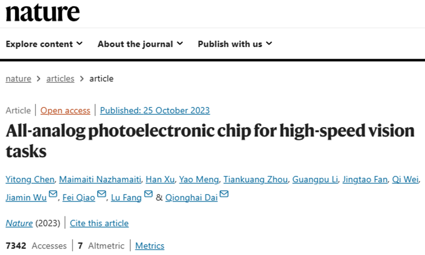
This October, two papers published in Nature injected fresh hope into the field: On October 19, a team led by Oxford University professor and Royal Academy of Engineering Fellow Harish Bhaskaran demonstrated a photonic in-memory computing architecture for the first time, opening a new pathway to enhance parallelism in photonic processors. On October 25, a team led by Academician Qionghai Dai at Tsinghua University built on a purely analog optoelectronic fused computing architecture to create another ultra-high-performance optoelectronic chip — ACCEL.
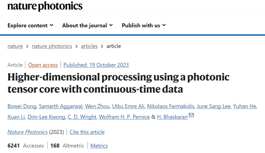
The Oxford team introduced a cutting-edge integrated photonic-electronic hardware capable of processing three-dimensional (3D) data. This "high-dimensional" processing results from encoding data across multiple radio frequencies — a breakthrough that not only meets the escalating demands of modern AI tasks but also elevates computational parallelism to unprecedented levels. In a practical application, the team deployed this novel hardware to assess sudden cardiac death risk from electrocardiograms of heart disease patients. The results were striking: the system successfully analyzed 100 ECG signals simultaneously with an impressive accuracy of 93.5%.
First author Dr. Bowei Dong of Oxford's Department of Materials emphasized the paradigm shift their findings represent. "Using radio frequencies to represent data opens another dimension," he noted, "enabling ultra-high-speed parallel processing for emerging AI hardware." It not only addresses the escalating demand for processing power in groundbreaking fashion, but also lays the groundwork for unprecedented possibilities, heralding a new era for AI hardware processing where the convergence of space, wavelength, and RF frequency will unleash far-reaching waves of innovation.
Meanwhile, the Tsinghua team creatively proposed a deeply integrated optoelectronic computing framework. Based on a purely analog optoelectronic fused computing architecture, this chip demonstrated — in real-world tests on intelligent vision tasks including ImageNet — thousands of times greater computing power than existing high-performance GPUs at equivalent accuracy, with four million times better energy efficiency. Going further, the chip's optical components were fabricated with minimum line widths at the hundred-nanometer scale, while the circuit portion used only 180nm CMOS process technology — yet achieved performance improvements of multiple orders of magnitude over 7nm high-performance chips.
These two papers achieved optical computing breakthroughs through different pathways. Combined with the fact that optical operations can be performed with virtually no dissipation, it is reasonable to expect that optics is becoming highly competitive in surpassing electronics.
2
Seventy Years of Optical Computing
For decades, optical computing has been a well-defined field: with its own specialized conferences, scientific journal columns, and dedicated research programs and funding. This research area has also been called optical information processing, while terms like information optics or information photonics are now frequently used — all reflecting the field's evolution.
From the outset, the potential of optics for computing has faced considerable skepticism, while the potential and future of electronics went unquestioned. H.J. Caulfield wrote a paper in 1998 on the prospects of optical computing, discussing the competition between optics and electronics, and identifying three stages: first, "ignorance and underestimation" of electronics; then "awakening and fearful inferiority"; and now, "realistic acceptance that optical computing and electronics are eternal partners."
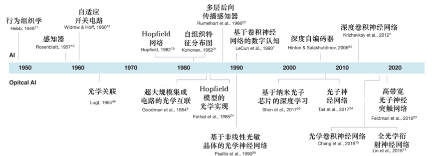
Timeline of milestone events in the development of AI and its corresponding optical implementations
The Fourier transform property of lenses forms the foundation of optical computing. Using coherent light, a lens performs a Fourier transform at its back focal plane of a two-dimensional transparency placed at its front focal plane. The processor consists of three planes: input, processing, and output. The processing plane may comprise lenses, holograms (optically recorded or computer-generated), or nonlinear elements, and will implement electro-optical conversion — which can be accomplished by a spatial light modulator (SLM).
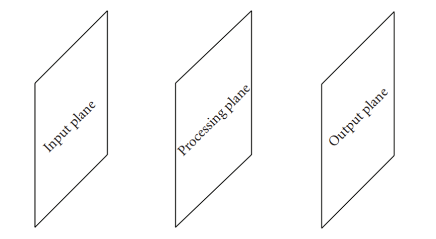
Architecture of a general-purpose optical processor for information processing. The processor consists of three planes: input, processing, and output.
The overall processing speed is limited by its slowest component, which in most cases is the input plane SLM, as most operate at video rates. The SLM is a critical component for developing practical optical processors, but unfortunately also one of the weakest links. Indeed, due to poor SLM performance and high cost, optical processors for real-time applications remained difficult to manufacture.
Information optics has been a recognized branch of optics since the 1950s. In fact, concepts from communications and information theory form the foundation of optical information processing. The invention of the coherent light source — the laser — in 1960 rapidly accelerated optical information processing, and all major inventions in this field were completed before 1970. By the early 1970s, enthusiasm for optics and information processing ran high; the potential of optics for real-time data processing appeared substantial. However, due to technical problems, particularly with SLMs, real-world optical processors remained rare. Research in the 1970s grew more pragmatic, with attempts to build optical processors for practical applications; competition with computers also intensified due to advances in computing. By the late 1970s, despite enormous research efforts, no SLM truly suitable for real-time optical information processing had emerged.
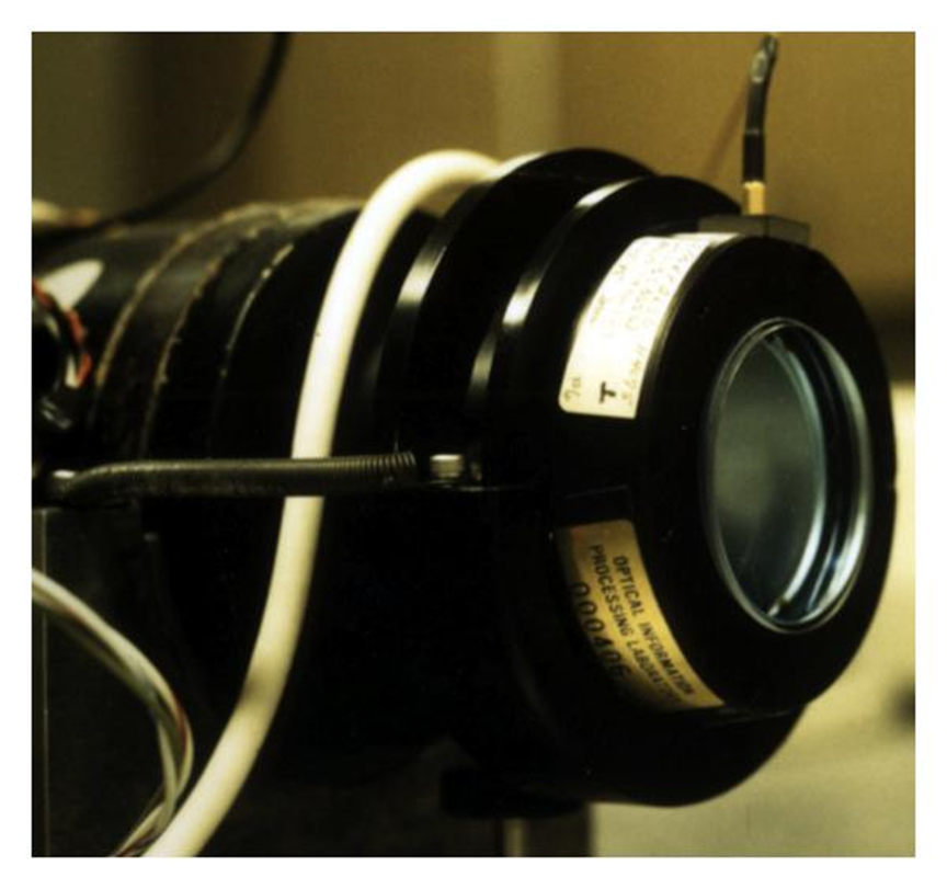
128×128 electrically addressed liquid crystal SLM, manufactured by French company LETI in 1975.
At the time, nearly all proposed processors remained laboratory prototypes, never given the opportunity to replace electronic processors — even though electronic and computing capabilities were far weaker than today. Many factors contributed to this: the number of applications that could benefit from optical processor speeds may have been insufficient, but the primary reason was the lack of powerful, high-speed, high-quality, affordable SLMs (for both input and filter planes of processors).
From 1980 through the early 2000s, optical research was extraordinarily intensive worldwide. In the 1980s, the technological landscape shifted: computers gained larger memory capacities, electron-beam writers became more widely adopted, and academic interest in neuromorphic computing surged. Because the availability of spatial light modulators was a critical bottleneck for optical information processing, substantial effort was devoted after 1980 to developing SLMs that could meet optical processors' demands for speed, resolution, size, and modulation capability.
In the 1990s, the major advance came in manufacturing methods with the adoption of photolithography. Thanks to progress in lithography, submicron-scale DOEs could now be fabricated — including polarization-selective CGHs, artificial dielectrics, and spot array generators.
Over the past two decades, optical processing and optical pattern recognition research entered another intensive phase. Every aspect of these processors has been investigated, with significant advances. Optical and photonic computing systems have made tremendous strides, opening entirely new opportunities in optical image classification, microscopy applications, imaging, and speech recognition.
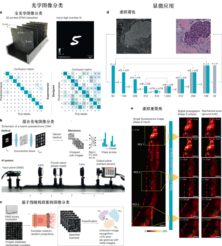
Applications of photonic deep learning in image classification and microscopy
The history of research in optical computing reveals an extraordinary scientific expedition. It began with the processing capabilities of coherent light, particularly its Fourier transform properties. This history demonstrates the enormous effort invested in building optical processors capable of real-time processing of massive data volumes. Today, optical technology dominates telecommunications — including optical fiber and cable, wavelength-division multiplexing (WDM), optical amplifiers, and MEMS-based switches. Over more than half a century of development, optical and photonic computing systems have advanced tremendously and have explored innovative solutions to some of the most challenging problems: all-optical nonlinearity, reliable control of large-scale photonic networks, electro-optic conversion efficiency, and programmability.
3
Two Nature Papers:
Breakthroughs Through Different Paths
Photonic systems can leverage a large number (>10^6) of parallel spatial modes. Consumer electronics using >10^8 spatial modes across an area of roughly 2.5 cm^2 have already been demonstrated, showing that massive parallelism is practically achievable. In a paper published in Nature Photonics on October 19, the Oxford University team led by Harish Bhaskaran provided another pathway for improving photonic processor parallelism by introducing RF modulation of photonic signals: alongside spatially distributed non-volatile memory and wavelength multiplexing, this added an extra dimension to the data; using high-dimensional processing techniques, the system was configured into an architecture compatible with edge computing frameworks. By validating the feasibility of continuous-time data computation in the optical domain, the system achieved a parallelism of 100 — two orders of magnitude higher than implementations using only spatial and wavelength degrees of freedom.
These preliminary projections offer an enticing prospect: even with judicious tuning of input and output parameters, this avant-garde approach can yield an incredible 100-fold amplification in energy efficiency, eclipsing the performance of existing state-of-the-art electronic processors. Most importantly, 100-fold parallelism is not the ceiling; if lower precision is permitted, up to 150 RF components can be multiplexed. Using 16 wavelength-division multiplexing channels, overall parallelism of 2,400 can be achieved, suggesting that a single system could synchronously process signals from 2,400 terminal devices — something impossible with existing low-dimensional processing technologies.
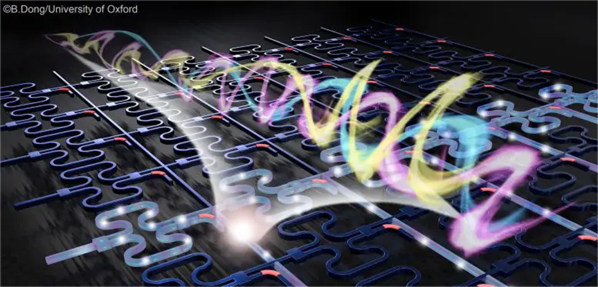
Artistic rendering of a photonic chip with data encoded in both optical and RF frequencies
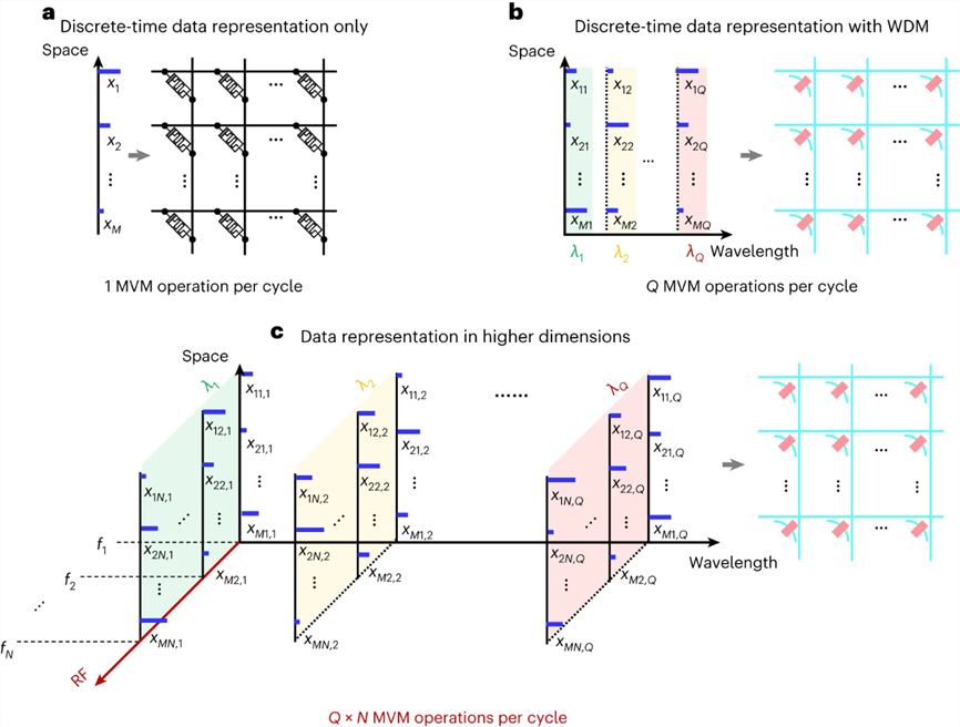
Oxford University team's high-dimensional photonic in-memory computing
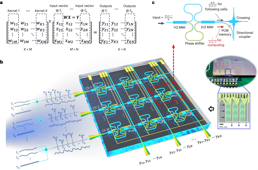
Schematic of multi-dimensional photonic computing-in-memory chip
Today, silicon photonic integrated circuits have found applications in on-chip optical sensing, quantum optical computing, and optical neuromorphic computing, and are regarded as a candidate technology for next-generation computing systems. They can boost electro-optical transmission speeds and address the signal loss and heat dissipation problems encountered with copper interconnects in current computer components. Consequently, semiconductor giants including TSMC and Intel have invested in related R&D. However, current silicon photonic logic devices suffer from relatively high insertion loss, and cascading multiple devices produces substantial optical attenuation. To mitigate these issues, the representative solutions adopted by different labs are phase-change materials (PCM) and Mach-Zehnder interferometers (MZI).
MZI optical switches implement all-to-all optical interconnection within the plane. By adjusting voltage values, the splitting ratio of MZI optical switches is controlled, enabling programmable weight matrices to be loaded onto the chip. In this scheme, the number of neurons in an adjacent layer that any single neuron in a given layer can connect to is limited, and the MZI wiring characteristics lead to poor scalability; the phase shifters are thermo-optically controlled, resulting in substantial energy loss. Although the MZI architecture is being adopted by most other companies, these are technical issues that require focused attention in subsequent development.
Phase-change materials (PCM) are alloy materials doped with semiconducting elements such as germanium, selenium, and antimony. Various PCM series produced through different formulations and processes are widely used in industry. Compared to pure silicon materials, phase-change materials are superior modulation materials: to achieve equivalent or even better modulation effects, chip area and required modulation electrodes are less than one-tenth of pure silicon solutions, dramatically improving photonic chip integration density and manufacturability. Meanwhile, phase-change materials exhibit excellent non-volatile storage characteristics and are low-cost. In this context, "phase change" does not refer to light but to the material's properties: when the material is in amorphous state, its transmittance is higher than in crystalline state. PCM exists in two distinct states — when amorphous, it shows high transmittance and light waves can propagate through; when crystalline, it exhibits low transmittance and most light waves are absorbed by the material and cannot pass through. Overall, when applied to light modulation, thanks to the properties of phase-change materials and combined with unique designs in devices, chip architecture, and light modulation, the advantages of the PCM-based optical computing approach are more readily quantifiable. PCM's decades of widespread industrial application have proven the material's reliability and stability, yet in optical computing applications, breakthroughs are still needed in sustained, efficient, and reliable control of this material. This time, after ten years of cultivation and breakthroughs, the Oxford University team has successfully demonstrated a commercially viable photonic in-memory computing architecture through phase-change optical computing technology, achieving comprehensive performance improvements in integration density, power consumption, stability, and latency — potentially greatly accelerating the commercialization of optical computing chips.
The other major implementation approach for photonic circuits, corresponding to silicon photonic computing (chips), is spatial light diffraction computing (devices): building computational capability directly into light fields propagating through free space or some medium. The foundation of spatial light computing is the method based on optical correlators proposed by Vander Lugt in 1964. Computation is achieved through spatial filtering: a matched filter is placed at the system's focal plane to perform phase compensation on the input optical signal, producing an optical signal at the output plane representing the computation result. This approach has several issues requiring subsequent focused attention: for example, pixels are too large, resulting in small fan-in/fan-out angles and weak connectivity; high integration density cannot be achieved in the short term; using spatial light modulators to load matrix elements entails high power consumption and slow refresh rates; fixed dielectric materials are non-tunable; and computational functions are simple.
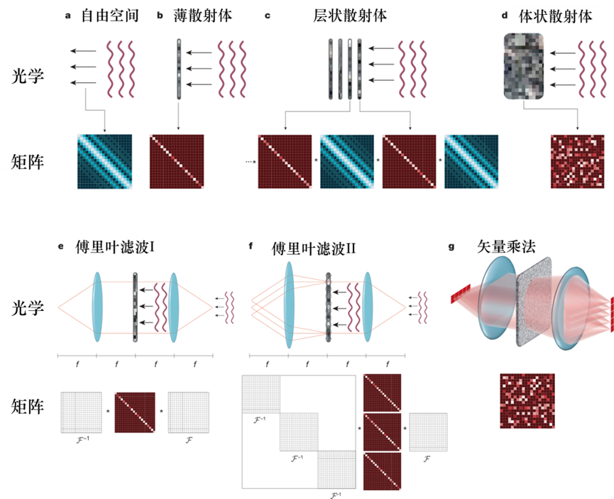
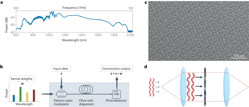
Light propagation in different media and corresponding linear matrix operations
The deep optoelectronic fusion computing framework creatively proposed by the Tsinghua University research team falls precisely within this domain.
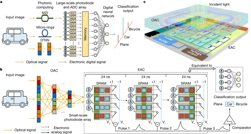
ACCEL architecture
In intelligent vision tasks and traffic scenario computing demonstrated by the R&D team, the system-level energy efficiency of the optoelectronic fusion chip (operations per unit energy) reached 74.8 Peta-OPS/W in actual measurements — more than 4 million times that of existing high-performance chips. As the researchers put it: "To put it vividly, if the original power supply could support existing high-performance chips for one hour, the same power supply would allow the ACCEL chip to operate for over five hundred years."
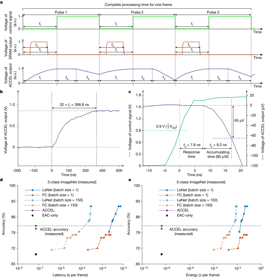
Experimental measurements of ACCEL processing time and energy consumption
The Tsinghua University R&D team's work integrates spatial light diffraction computing with analog electronic chips, experimentally demonstrating the superiority of optoelectronic analog hybrid computation — achieving substantial improvements in data throughput, computational energy efficiency, and processing latency. For vision tasks in AI computation (such as convolution), the spatial light diffraction approach is an excellent choice.
What this approach lacks, however, is the fact that spatial light computation inevitably requires light to travel a certain distance, so the hardware footprint remains relatively large. Integrated optical computing faces no obvious constraints on input data size or the linear operations it performs, and it offers advantages in size and integration density — computation can be executed at the micrometer scale. Moreover, silicon-photonics-based integrated optical computing is configurable and programmable, capable of meeting the demands of large-scale complex AI computation such as large model inference and training. Spatial light computing, by contrast, can currently handle only convolution tasks in its optical domain and lacks processing capability for other data types like audio and text. Additionally, from an industrial maturity perspective, this approach must also contend with the cost of spatial light modulator arrays and the need to validate its efficiency for tasks beyond visual information processing.
With the ultra-high-performance optical chips proposed by these two research teams, the birth of the "computer of the future" no longer seems distant. These novel architectures will not only carve out a new path for this future technology to reach everyday life, but also offer deep inspiration for the integration of other future high-efficiency technologies — quantum computing, in-memory computing — with current electronic information systems.
Perhaps the emergence of these chips will bring next-generation computing architectures into daily life far sooner than anticipated.
Optical Computers Are Gradually Becoming Commercialized
In fact, they have already entered our daily lives. Over the past several decades, optical devices have been released as commercial products multiple times. Commercially, this is already a vibrant, thriving domain.
In 2022, Hewlett Packard Enterprise (HPE) signed a multi-year strategic partnership with photonic computing startup Ayar Labs to accelerate network performance in computing systems and data centers by developing silicon photonic solutions based on optical I/O technology. Shortly thereafter, news emerged that Ayar Labs had secured an additional $130 million in funding from multiple new and existing investors including HPE, NVIDIA, and Intel Capital.
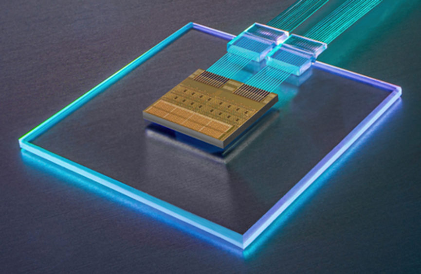
In March 2023, Ayar Labs demonstrated the industry's first 4-Tbps optical solution
Founded in 2018, Israeli company Cognifiber takes a novel approach to solving optoelectronic interconnects. The solution abandons silicon photonics entirely in favor of glass in the form of multi-core optical fiber. The idea is to use interference between cores to simulate the interactions between neurons and synapses in multi-layer neural networks.
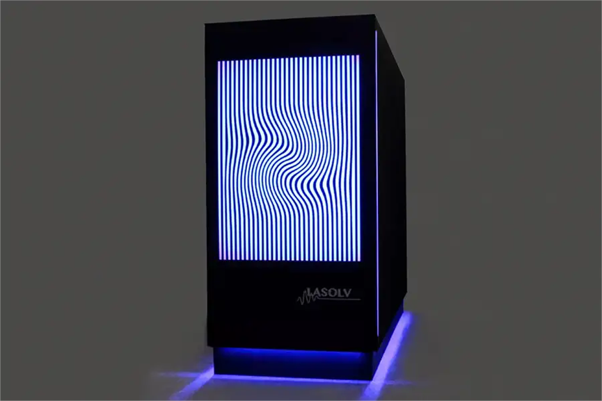
Japan's NTT is building precision optical computers
Japanese company NTT is also developing an optical computer believed to outperform quantum computing in solving optimization problems. To date, Chinese quantum physics teams have also announced multiple light-based quantum computing achievements. Other companies such as US-based Honeywell and IonQ are using trapped ions to tackle this challenge.
Domestic commercial players in this field already exist. Founded in 2022, Guangbenwei Technology (光本位科技) has raised over 50 million yuan in angel funding, completed multiple tape-outs, achieved optoelectronic co-packaging, and validated its algorithms. The company has established long-term strategic partnerships with multiple upstream and downstream industry players to collaborate on rapidly bringing optical computing to full industrialization. Replacing electricity with light in the computing domain is a systematic engineering endeavor requiring the mobilization of substantial industry chain resources. Guangbenwei's core technology leverages the unique advantages of phase-change materials — small unit size and low energy consumption — to rapidly scale optical computing to commercial-grade computing power of 128×128, 256×256, 512×512, and beyond. These large-scale chips can already achieve end-to-end performance tens of times greater than NVIDIA's AI chips, with future expected performance advantages of 1,000–10,000× over current electronic chips. Guangbenwei's optical computing products are expected to rapidly enter people's lives alongside the explosion and maturation of large models.
Guangbenwei's founding R&D team originated from Oxford University's Bhaskaran Lab. The Bhaskaran Lab is named after Oxford University Materials Professor and MPLS (Mathematical, Physical and Life Sciences Division) Associate Head Harish Bhaskaran. Professor Bhaskaran is dedicated to optoelectronic integration research using nanoscale phase-change materials, and is a pioneer and founder of phase-change material nanophotonics and phase-change photonic computing, advancing the scientific and industrial progress of large-scale computing power, low power consumption, and high-performance photonic computing. In September 2023, Professor Harish Bhaskaran was elected a Fellow of the Royal Academy of Engineering in recognition of his outstanding contributions to nanomaterial applications and advanced nanoengineering technology. During his ten years at Oxford, Professor Bhaskaran published 18 high-impact papers in Nature and Science and their subsidiary journals, accumulating over 10,000 citations. His main research directions include photonic computing, photonic memory, neuromorphic computing, and high-performance phase-change materials.
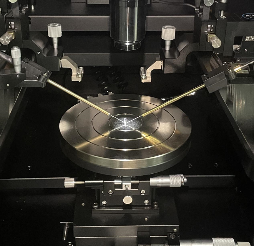
Guangbenwei Technology R&D platform and chips
Lightelligence, founded in 2017 and based on MIT's MZI technology path, maintains offices in Boston and Shanghai. Four years after its founding, it released a chip called PACE containing approximately 10,000 photonic devices and a microelectronic chip providing control and memory. A single PACE chip carries about 12,000 photonic devices and has currently completed demonstrations of specific Ising models, with speed outperforming NVIDIA's RTX 3080. Following the release of the PACE optical computing prototype, Lightelligence is now heavily investing in optical interconnects, optical communications, and other domains. Envise achieves three times the inferences per second on the largest neural networks compared to NVIDIA's DGX-A100, and seven times the inferences per second per watt on BERT-Base using the SQuAD dataset compared to NVIDIA's DGX-A100. In May this year, Lightmatter secured $154 million in Series C funding to deliver photonic products to customers.
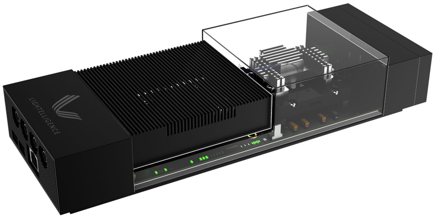
PACE optical computing prototype
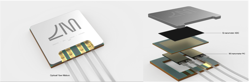
Lightmatter Envise optical processor chip
Overall, the global photonic computing chip industry has just begun and holds tremendous market potential. Pioneers who master core technologies and deeply understand industry dynamics will lead China to accelerate toward an era of optical computing — a chance to overtake on a different track.
"Optics In, Copper Out" — The Future Is Already Here!
As commercialization gradually advances, we are already seeing achievable applications for photonic computing in near-edge computing and data centers. This means that with near-edge computing capabilities, 5G-enabled IoT devices in retail stores can compute and store some of the data they generate rather than transmitting all raw data to distant data centers — leveraging the low latency and low transmission loss advantages of photonic computing.
Compared to electronic computing, photonic computing offers dramatically improved energy efficiency ratios. At equivalent clock frequencies and power consumption, photonic computing delivers computational throughput more than 100× that of electronic computing, meaning substantial reductions in energy consumption. Rough estimates suggest this could save data centers over 70% in annual electricity costs, equivalent to hundreds of millions of yuan in savings.
As demand for large-scale, high-computing-power scenarios such as AI and cloud computing grows rapidly, photonic computing chips still have enormous room for performance improvement, helping to more quickly fill the global gap between AI computing supply and demand. After the US imposed multiple rounds of sanctions on China's electronic chip industry, we face not only direct cutoffs of cutting-edge AI chips but also comprehensive supply chain shortages of high-end manufacturing equipment and design software. And with the bottleneck of Moore's Law arriving for electronic chips, this development constraint is nothing short of compounding the damage — electronic chips may have already reached their performance limits.
For photonic computing, however, future techniques such as wavelength-division multiplexing and frequency-division multiplexing can enable hundred-fold or thousand-fold performance improvements. We can simply imagine this as the "Moore's Law of light" — it has only just begun. And achieving a near-perfect photonic computing product is far less difficult than imagined: tape-outs can be completed using only 180nm/130nm process lines retrofitted from CMOS production lines, with overall manufacturing costs more than 80% lower than electronic chips.
Despite technical difficulties, various integrated photonic computing architectures have been proposed and applied to solving NP-hard problems or executing machine learning tasks. Considering long-term development, large-scale reconfigurable photonic circuits are essential. Signal attenuation of light in large-scale computation may significantly impact computational results. To address these limitations, the application of single-photon detectors and quantum detection technologies could substantially enhance the scale of photonic computing that can be processed in reality. Through the unremitting efforts of the scientific and industrial communities, in the foreseeable future, optical computing will rapidly improve integration density and computational performance, effectively complement electronic computing, and greatly enhance the comprehensive performance of hybrid computing systems.
With the arrival of the information age and the artificial intelligence age, advanced photonic technologies and cutting-edge quantum technologies have opened a new chapter for light-based computing, bringing optical computing into the race. Viewed this way, "optics in, copper out" may indeed be the natural course of development.
In China, senior scientists such as Gong Zutong and Qian Xuesen had already been calling frequently as early as the late 1970s for vigorous development of photonics as an academic discipline. Professor Qian Xuesen proposed that "photonics is a science parallel to electronics," and he was the first to propose a development model for photonics of "photonics — photonic technology — photonic industry." Today, China's Xi'an Institute of Optics and Precision Mechanics (CAS), Institute of Microelectronics (CAS), Institute of Semiconductors (CAS), Shanghai Institute of Microsystem and Information Technology, as well as Fudan University, Shanghai Jiao Tong University, Tsinghua University, Zhejiang University, and Huazhong University of Science and Technology have all conducted long-term research. The state has also implemented a series of major research programs targeting photonic integration technology, achieving substantial accomplishments in this domain.
The laws of natural evolution and the trajectory of technological progress both follow discernible patterns. Light replacing electricity is a form of "dimensional reduction strike" — one that has already displaced and surpassed electrical solutions in virtually every corner of human life. The past decade of research and industrial development in optical computing has laid the groundwork for its comprehensive commercial deployment, beginning now and unfolding over the coming years.
References (scroll to see more):
[1]https://www.bis.doc.gov/index.php/about-bis/newsroom/2082
[2]https://readwrite.com/the-rise-of-photonics-in-computing-next-big-thing-for-deeptech-vcs/
[3]https://www.nature.com/articles/s42254-023-00645-5#citeas
[4]https://www.hindawi.com/journals/aot/2010/372652/
[5]https://ieeexplore.ieee.org/document/652905
[6]https://www.nature.com/articles/s41566-023-01313-x
[7]https://www.nature.com/articles/s41566-023-01217-w
[8]https://www.nature.com/articles/s41586-023-06558-8
[10]https://www.eejournal.com/article/are-we-poised-to-turn-the-optical-computing-corner/
[11]https://news.cnstock.com/industry,rdjj-202308-5101848.htm
[14]https://www.nature.com/articles/s42254-023-00645-5
[15]https://mp.weixin.qq.com/s/1FJnMQm3cmGOb40T-PPmJg
[16]https://opt.cas.cn/kpyd/gxqy1/gxlw1/201110/t20111007_3359009.html
[17]https://lw.news.cn/2022-01/10/c_1310416707.htm
[18]https://arxiv.org/abs/2305.15820
[19]https://nanoeng.materials.ox.ac.uk/people/harish-bhaskaran
[20]https://nanoeng.materials.ox.ac.uk/home
[21]https://mp.weixin.qq.com/s/1Gs2o5BRS5o8uwh2NCQKzQ
[22]https://mp.weixin.qq.com/s/MsL1MKanuRZH6BrSqHUyuQ
[23]https://www.nature.com/articles/s41586-020-2973-6
[24]https://mp.weixin.qq.com/s/f5zQQNRBOUOZ_ETjZc6WFQ