Garen Semiconductor Closes Nearly RMB 100 Million Pre-A Round, Announces Strategic Partnership with Hangzhou Bank | BlueRun Ventures
From successfully achieving 6-inch cast-grown single-crystal ingots, to breaking through 3-inch wafer-scale (010) substrate fabrication technology.
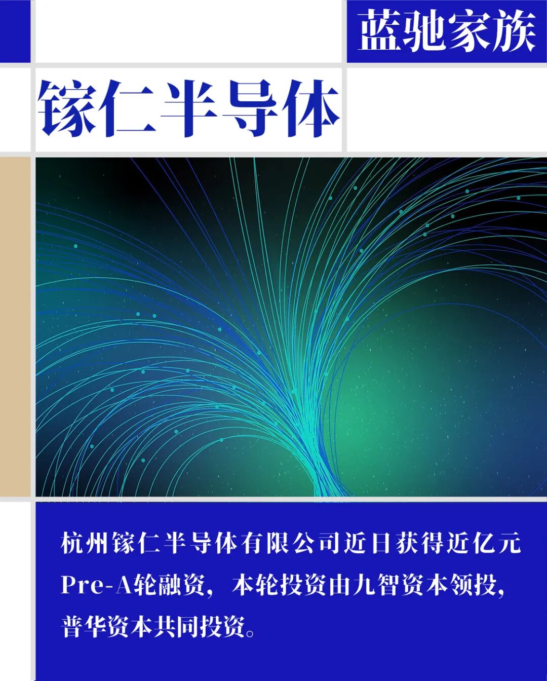
Hangzhou Jaren Semiconductor Co., Ltd. recently secured nearly 100 million RMB in Pre-A funding, led by Jiuzhi Capital with Puhua Capital as co-investor. This capital injection represents not only strong recognition of the company's technical capabilities and market prospects, but also provides solid financial backing for its future growth.
Alongside this, the signing of a strategic cooperation agreement with Hangzhou Bank will enable the company to deepen its collaboration with financial institutions, jointly exploring new models and pathways for the deep integration of technology and finance — injecting fresh momentum into its sustained and rapid development.
BlueRun Ventures led Jaren Semiconductor's angel round.
Since its founding in September 2022, Jaren Semiconductor has focused on ultra-wide bandgap semiconductor gallium oxide (Ga₂O₃) single-crystal materials, supplying customers with gallium oxide semiconductor substrates and epitaxial wafers in various sizes and crystal orientations. In just over a year, the company has achieved a series of technical milestones, from successfully demonstrating 6-inch casting-method single-crystal growth to breaking through 3-inch wafer-level (010) substrate preparation technology.
The company's founding team hails from Zhejiang University's State Key Laboratory of Silicon Materials and the Zhejiang University Hangzhou International Science and Technology Innovation Center. It has now assembled an R&D and production team with a Chinese Academy of Sciences academician serving as chief advisor, and will continue to provide material support for the development of China's power electronics and related industries.
As a fourth-generation semiconductor material, gallium oxide offers excellent performance characteristics and broad application prospects. The Jaren Semiconductor team brings strong research backgrounds and industrialization experience, with fully independent intellectual property rights across multiple core technologies. Its self-developed casting method features significant advantages in cost, material loss, and process controllability, and will provide meaningful support for China's competitiveness in the global technology arena. The company is also carrying out a series of dedicated R&D programs that will prove significant in driving innovation and performance improvements in next-generation electronic devices.
Yang Deren, academician of the Chinese Academy of Sciences and chief advisor to Jaren Semiconductor, stated that this funding round will accelerate the industrialization of gallium oxide materials and devices, injecting new impetus into the development of related industries. The Jaren Semiconductor team will actively promote the cultivation and development of new quality productive forces, tackling the "bottleneck" challenges in semiconductor materials, and contributing to China's pursuit of self-developed core industrial technologies.


HKIC Partners with Galaxy Universal to Expand Hong Kong Ecosystem: AI-Powered Humanoid Robots Interact On-Site, Embodied Intelligence Draws Tech Talent | BlueRun Ventures Headlines
$200M in Sales Within Two Years of Founding: Viture Tops Amazon's Smart Glasses Category | BlueRun Ventures Headlines
Using AI to Shorten Metal Materials R&D Cycles: DeepMaterial Lands Orders from Leading New Energy Vehicle Makers | BlueRun Ventures Headlines