Can Domestic Semiconductor Materials Outpace International Competitors? | FreeS Fund Chip Series

How Can China's Semiconductor Industry Break Free From the "Chokehold" Dilemma?
From a macro perspective, the semiconductor industry's growth trajectory looks promising. In October 2021, the Semiconductor Industry Association announced global semiconductor sales of $48.8 billion for the month, up 24.0% year-over-year. But for China's semiconductor professionals, this international growth can't mask the supply chain chokehold they're experiencing. From the U.S. National Security Commission on Artificial Intelligence's (NSCAI) treaty restrictions targeting Chinese chip technology, to the Donald Trump administration's explicit export controls on SMIC, these disruptions have been battering China's semiconductor supply chain.
With upstream supply chains constrained, Chinese semiconductor professionals have had no choice but to go it alone, and "domestic substitution of semiconductor materials" began appearing frequently in industry discussions. But is this path to domestic substitution viable? And if so, how? These are questions many in the industry are eager to answer.
Recently, FreeS Fund invited a semiconductor materials entrepreneur — Lou Xiabing, co-founder of YuanGui Materials Technology. Lou holds a B.S. in chemistry from Fudan University's elite science program and a Ph.D. in chemistry from Harvard University, where he studied under Professor Roy Gordon, a member of both U.S. national academies. Since co-founding YuanGui Technology in 2020, he has focused on solving the chokehold problems in semiconductor nanofilm materials.
Drawing from his observations and research on the semiconductor materials industry in recent years, he discussed the following topics with the audience:
- What notable inflection points have shaped the industry recently?
- How should we understand the relationship between semiconductor materials and wafer fabrication?
- Can domestic semiconductor materials match or surpass international standards?
- Where should semiconductor materials companies go from here?
This is the second installment in FreeS Fund's chip series. We hope it offers some useful insights.
Engagement Perks: We warmly welcome your thoughts in the comments section. The three most thoughtful commenters will receive a custom FreeS Fund notebook set (including two notebooks in different styles). Comment screening closes at 12:00 PM, April 6, 2022.


/ 01 / Three Milestones That Shaped the Industry
It's a great honor to have this opportunity to discuss topics that have been generating considerable buzz in our industry, both domestically and internationally. First, let me introduce what YuanGui Materials Technology aims to do: we want to develop domestic substitution products in the upstream raw materials sector of China's semiconductor industry. Whether this is feasible, and if so, how — that's what I'd like to talk about today.
Before diving in, let me walk you through three industry-related news events.
▍The Trend Toward Industry De-globalization
In July 2019, Japan imposed strict semiconductor export restrictions on South Korea. The upstream raw materials primarily affected included fluorinated polyimide (used in smartphone screens and OLED panel manufacturing), photoresist, and high-purity hydrogen fluoride (used in semiconductor manufacturing). Because of their inherent properties, these three materials are difficult to stockpile in large quantities over extended periods, making such upstream trade restrictions devastating to downstream manufacturing.
This Japan-Korea semiconductor raw materials trade dispute made the industry realize something: we had assumed the semiconductor industry was one where countries worldwide freely collaborated and shared supply chain resources to reduce costs. But this trade dispute served as a wake-up call — every enterprise and country needs to plan ahead and keep supply chain security in its own hands. Otherwise, as with Japan and Korea, when goodwill evaporates, upstream and downstream regions can use supply chain chokeholds as bargaining chips, inflicting massive damage on the industry.
This is what I consider a milestone event for the semiconductor industry — the first time it triggered a de-globalization trend.
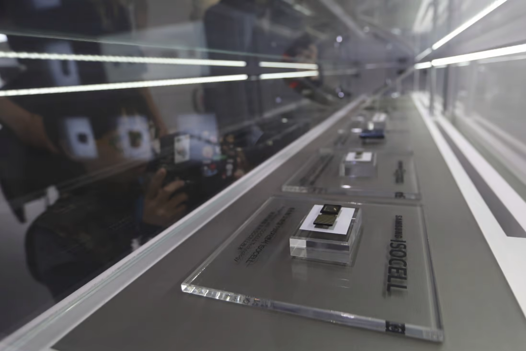
Samsung microchips on display in Seoul, South Korea. Japan is the dominant supplier of materials used in most of the country's computer chip equipment. | AP
▍China's Semiconductor Industry Under Assault
The second news item is more directly relevant to our domestic industry. In the second half of 2021, the Donald Trump administration imposed new export restrictions on SMIC, China's most advanced computer chipmaker. This meant that after that point, any equipment or raw materials SMIC purchased from the United States required approval from the Ministry of Commerce of the People's Republic of China, with particular scrutiny on equipment critical to advancing China's most cutting-edge chip process technology, such as EUV (extreme ultraviolet) lithography machines.
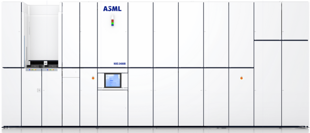
The world's most advanced ASML EUV lithography machine. Lithography processes at approximately 7nm and below require machines of this caliber. Unit price: roughly $150 million. | EUV lithography systems – Products | ASML
The implementation of these trade restrictions meant that SMIC would struggle to advance to leading-edge chip processes without international supply chain access, and China's semiconductor supply chain was consequently threatened. This was the industry's second milestone event.
▍Endless Debate Over Domestic Substitution
The third news item occurred in mid-2021, when a domestic listed company announced that its photoresist project had passed validation at a wafer fab. At the time, some financial industry analysts viewed this as an important signal that "domestic substitution" was about to enter the supply chain, a potential solution to the urgent problem of upstream supply chain chokeholds. But an authority in the semiconductor industry argued that domestic photoresist still had ground to cover in quality improvement, and the two sides clashed.
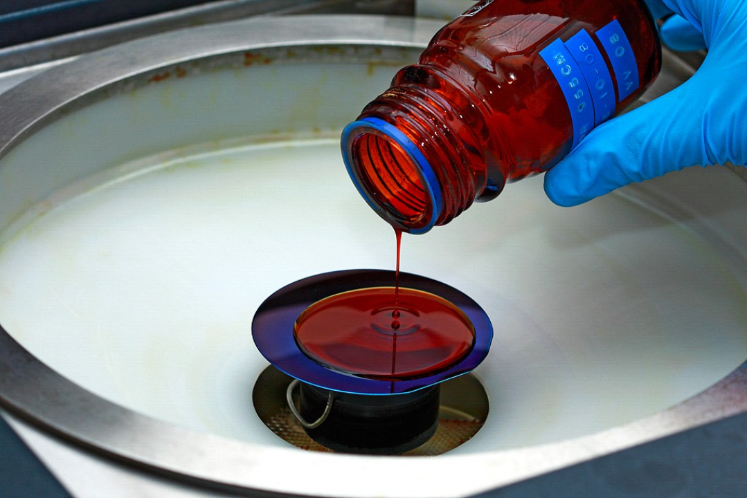
Photoresist, shown here in a laboratory-grade spin-coating process. | photoresist spin coating - Bing images
I won't take sides on this debate; I'll simply offer my personal interpretation.
First, for the industry, developing "domestic substitution" for photoresist materials is imperative — we must escape the predicament of having raw materials held hostage by other countries.
From a market and stock market perspective, people naturally want to hear about new developments and good news. But this can also lead to excessive optimism. From the perspective of industry technicians, we find that even if a material passes wafer fab validation, that doesn't mean it can immediately be put into production lines. There can be a huge gap in understanding between frontline technicians and those outside the industry.
This cognitive gap has spawned two starkly different viewpoints. One side believes that China's semiconductor raw materials, photoresist included, are on the verge of achieving "domestic substitution," and that we'll soon see fully domestic 28nm and even 14nm chips in mass production.
The other side argues that there's still a gap between China's current domestic production capabilities and the United States — like Zeno's paradox of Achilles and the tortoise. Though Achilles runs swiftly, the tortoise keeps moving forward. Thus our semiconductor industry cannot fully catch up to the global cutting edge, only approach it asymptotically.
So today, using these three news items as a starting point, I want to systematically discuss: first, can domestic semiconductor materials reach or surpass international advanced levels? Second, if they can, what opportunities can we seize? Third, as a semiconductor materials company, how can we actually make good materials?
/ 02 / What Are Semiconductor Materials? What Is Lithography?
But before tackling these questions, I want us to think together: "What is a semiconductor? What is lithography technology?"
Let's start with semiconductors. Textbooks used to define semiconductors as "materials whose electrical conductivity at room temperature falls between that of conductors and insulators." I find this description intuitive but not quite precise, because it doesn't capture the most critical characteristic of semiconductor materials. When we evaluate whether a semiconductor material is suitable as a raw material, the deciding factor usually isn't how strong or weak its conductivity is, but whether we can dramatically modulate that conductivity through a very simple or low-cost method.
Nearly all semiconductor materials on the market today have an extremely wide range of electrical conductivity. Within this range, we can change external conditions — such as voltage — to alter conductivity: increase voltage to raise conductivity, decrease voltage to lower it. It's like finding a switch for conductivity.
Sensors developed based on semiconductor materials exploit this property. Gallium arsenide, a common semiconductor material, is frequently used in sensors — higher light intensity means higher conductivity, lower intensity means lower conductivity, allowing us to design device operations accordingly. Whether we can effectively and flexibly alter a material's conductivity across a wide range — this, I believe, is the core of defining semiconductor materials.
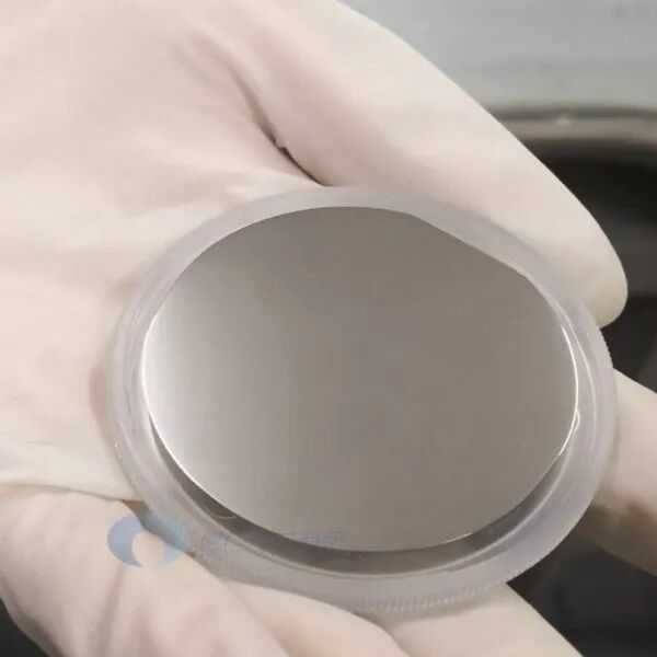
Gallium arsenide single-crystal wafer | Xiamen Sino-Crystal Research
Moreover, when many people think of semiconductor materials, they probably only think of silicon or gallium arsenide substrates. But in reality, turning raw semiconductor materials into finished devices requires thousands of different materials in between. Over the past few decades, the semiconductor industry's manufacturing precision has advanced step by step alongside Moore's Law. Today, we've reached 3nm chip process technology, and as processes have continued to evolve, the variety of semiconductor materials used has flourished as well.
So what is lithography? We can understand it as using a light source generated by a lithography machine to project specific patterns onto wafer materials, thereby creating semiconductor circuit diagrams.
Let's look at the wavelengths used by lithography machines across different periods of semiconductor industry development. In the earliest days, mainstream lithography machines used mercury lamps as their light source, producing G-line ultraviolet light at 436nm and i-line ultraviolet light at 365nm. Starting in 1999, excimer lasers appeared — such as KrF excimer lasers at 248nm and ArF excimer lasers at 193nm. By the time ArF excimer lasers emerged, semiconductor chip process precision had already reached the 90nm node.
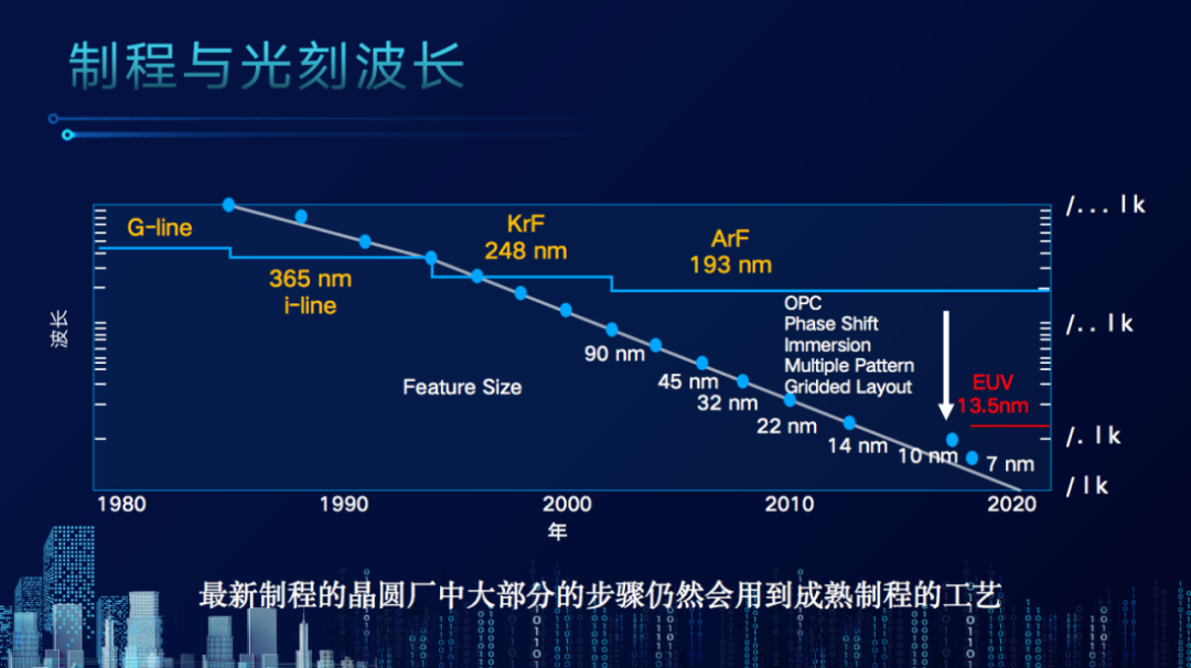
Process node and lithography wavelength | YuanGui Materials Technology
For a long time after that, lithography machines didn't see any revolutionary leaps forward. Yet chip process technology kept advancing — from 90nm to 45nm, 22nm, and then 10nm. During this period, despite the limitations imposed by lithography machine development preventing light source wavelengths from becoming even finer, semiconductor process engineers and materials engineers still achieved further shrinkage of chip processes through innovations in photoresist, thin film deposition, and numerous other process steps. This is both a testament to the industry's efforts and a crystallization of human ingenuity.
When chip processes reached the 10nm node, the industry had essentially exhausted the potential of 193nm deep ultraviolet light sources. So in 2016, EUV (extreme ultraviolet) lithography machines — frequently discussed today — finally emerged.
From that same year, the US-China trade dispute began. During this period, China attempted to purchase equipment from Dutch company ASML, which monopolizes the global EUV lithography machine market. But due to obstruction caused by the trade dispute, mainland China has not had a single EUV lithography machine to date. This means we currently cannot break through to chip processes at 10nm and below from the equipment side.
However, under the leadership of industry experts in China such as Liang Mengsong of SMIC, even without EUV lithography machines, there is considerable confidence that through our own efforts, we can push processes forward to 10nm.
/ 03 / Can domestic semiconductor materials reach or surpass international advanced levels?
Now let's formally discuss materials. What level have China's semiconductor materials reached so far?
To date, we can basically produce most semiconductor materials for the 90nm node and above domestically, with the exception of photoresist. Although for reasons of quality stability and other factors, most wafer fabs may not fully adopt domestic materials, we can confidently say that if upstream countries were to completely cut off supply, our domestic backup materials suppliers could essentially achieve substitution in these material areas.
What products do semiconductor materials for the 90nm node and above involve? They include most sensors, most power devices — such as gallium nitride devices used in phone chargers, or silicon carbide devices used in new energy vehicles, and so on. The semiconductor material processes for these devices are all above 90nm, and currently within this process range, basically all semiconductor materials except KrF photoresist can be produced domestically.
What does our company mainly do? ALD precursors — I'll elaborate on this shortly. They can be used in chip processes ranging from 45nm to the latest 3nm. We believe this process range is one that China will definitely break through in the future, making it an excellent direction.
If we simplify the entire chip processing workflow down to just the main steps, it's somewhat like building with blocks — combining and arranging individual modules together. The cross-section of the final structure looks something like this.
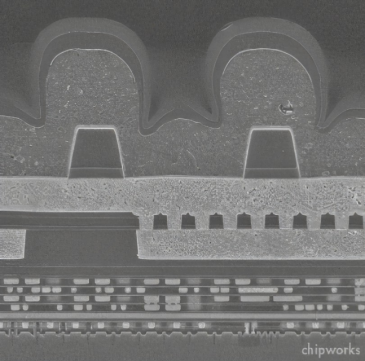
Cross-section of a chip | chipworks
The image shows the cross-section of Apple's A4 chip. I have to say, it really does resemble building blocks. How was it constructed? Explaining this process in the most accessible way, the workflow goes roughly like this:
Lay down a thin film at the very bottom of the chip → Use lithography to create a pattern on top (similar to the development step in early photography) → Use etching to carve and fix this pattern in place (similar to the fixing step in early photography) → Polish and smooth the surface → Repeat this process until the chip is complete.
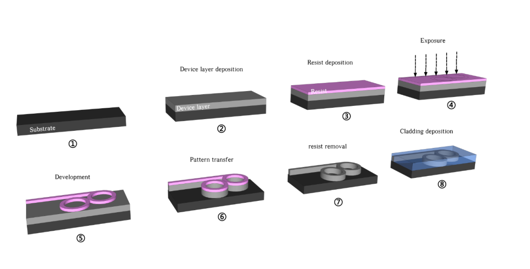
Simplified chip construction process
From the cross-section, we can observe that the lower layers of the chip are narrower, while the upper layers are wider. This means if a chip is labeled as a 22nm process, it indicates that the bottommost layer uses 22nm technology; going upward it might reach 90nm, and further up could even reach several microns. In other words, even companies with the most advanced chip process technology need equipment and materials that cover nearly all key process nodes leading up to their core process.
The chip production process involves various techniques including thin film deposition, lithography, etching, and chemical mechanical polishing. For China's current industry situation, each of these process steps involves equipment and materials that contain new entrepreneurial opportunities, because of the demand for "domestic substitution."
First, in the thin film deposition domain, the industry uses physical vapor deposition (PVD), chemical vapor deposition (CVD), and atomic layer deposition (ALD), among other processes. Atomic layer deposition is the main research direction of our company.
The materials used in these different deposition equipment include specialty gases, precursors, sputtering targets, and so on. Currently, there are already many domestic companies that have achieved results in developing specialty gases for CVD. ALD processes require precursors — this is our company's main product. Metal sputtering targets are what PVD needs, and domestic substitution in this area is already progressing quite well.
For lithography, the primary equipment is of course the lithography machine. In terms of the latest lithography equipment, China has not yet achieved international parity. In November, there were rumors that Shanghai Micro Electronics Equipment's 28nm lithography machine — more precisely, a lithography machine that could be used for 28nm chip manufacturing — failed national acceptance under the 02 Special Project*. This was unwelcome news for industry professionals, but we believe there will be breakthroughs in the coming years that will pave the way for domestic chip processes to enter the 28nm era.
Another very important piece of equipment in the chip manufacturing process is the cleaning machine. Its main function is to use cleaning solutions to remove residual photoresist, dust, and other contaminants from photomasks. Domestic substitution for this type of equipment is also progressing quite well. According to Qianzhan Research Institute data, the domestic substitution rate for China's semiconductor cleaning equipment has already exceeded 20%, far surpassing the average domestic substitution level for semiconductor equipment.
*: The "02 Special Project" refers to the "Very Large Scale Integrated Circuit Manufacturing Equipment and Complete Process" project. Because it was ranked second among the 16 major national special projects, it is known in the industry as the "02 Special Project."
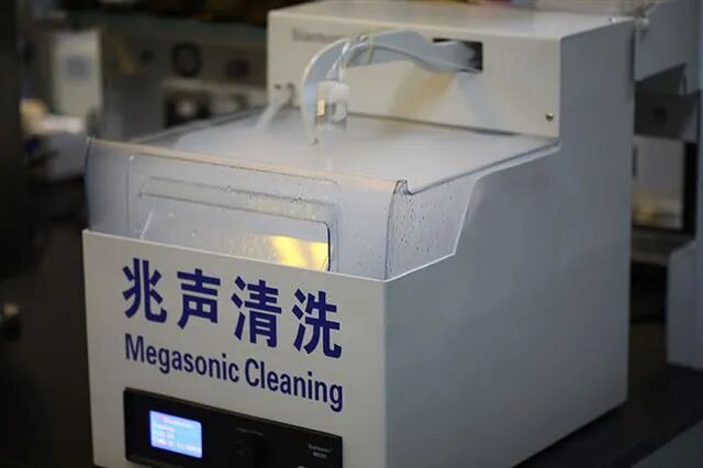
Domestic spray-type megasonic cleaning machine | Siansonic
Additionally, photoresist — one of the most critical materials for chip manufacturing — is also among the main hot topics in the industry market today. Photoresist quality has a direct bearing on yield rates and device performance. Currently, domestic substitution of photoresist is still ongoing. There was previously news that a company had successfully passed national acceptance for its 02 Special Project ArF photoresist, which can be used in integrated circuit manufacturing processes from 90nm down to 14nm and even 7nm technology nodes. However, there is still some distance to go before achieving mass production and application.
Another important material for lithography is the photomask, which is mainly used to create and precisely position various functional patterns on materials. The progress of domestic substitution here hasn't reached the level of cleaning machines yet, but it is advancing steadily.
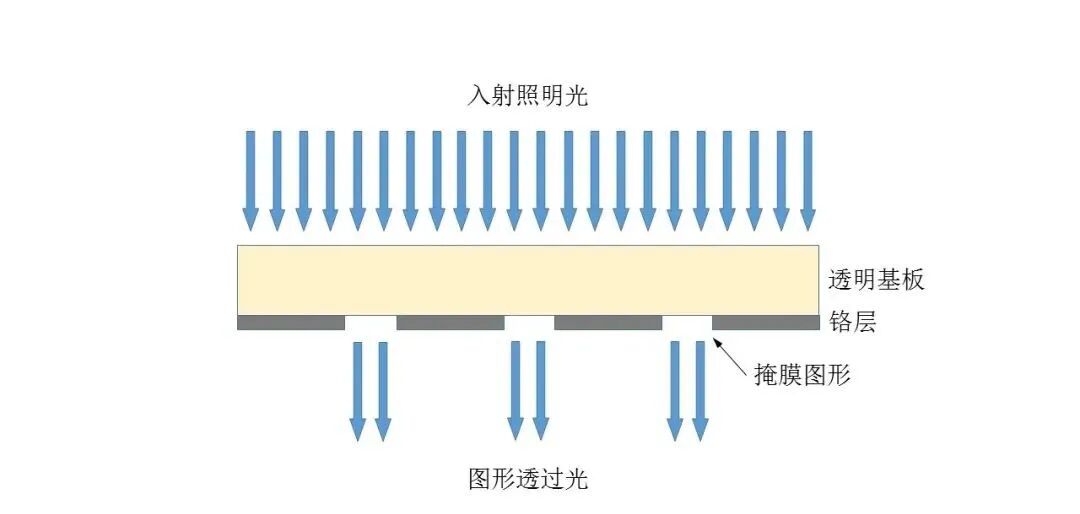
Photomask schematic | University of Science and Technology of China Micro/Nano Research and Fabrication Center
The etching step is particularly like sculpture — similar to when people carve stone tablets, where they paste a layer of paper on the stone surface and then chisel along the outline designed on the paper. That paper is the mask formed by photoresist on the substrate to be processed, and the etching machine is like the chisel that gradually carves the material along the mask pattern. Etching requires specialty gases, and China's capabilities in this area are already quite good for processes above 90nm, currently in a stage of seeking breakthroughs.
The final step is chemical mechanical polishing, much like the polishing step in a carpenter's work. Its purpose is to flatten the wafer surface to facilitate the next round of lithography. During polishing, some polishing slurry is needed as abrasive material, as well as a polishing pad (like sandpaper). Currently, our domestic polishing equipment still needs to achieve higher precision, but domestic substitution in the two areas of polishing pads and polishing slurry is progressing very rapidly, with domestic manufacturers quickly rising.
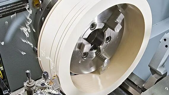
Grinding ring for chemical mechanical polishing | Ensinger Plastics
From the wafer fabrication process, it's not hard to see that materials and equipment are tightly intertwined. Developing a new material requires corresponding equipment for validation, and both materials and equipment serve the process together. This closely resembles the Wintel ecosystem we often talked about over the past two decades — every update to the Windows operating system required Intel to simultaneously boost CPU performance, and Intel's advances in process technology in turn spurred new generations of chip design architectures, creating a continuous positive feedback loop known as the Tick-Tock cycle.
The logic of our industry operates very similarly. When the industry develops a new generation of process technology, it creates new demands for both equipment and materials, forcing equipment makers and material suppliers to upgrade their processes or product varieties. Take chip manufacturing nodes: when moving from a 22nm wafer to 14nm, the equipment used for the bottommost, most precisely engineered layer must be upgraded, and the materials used there must be upgraded too. But the upper layers typically continue using previous materials and equipment. So while new process generations do involve equipment and material upgrades, this evolution usually only manifests at the bottommost layers of the wafer.
Returning to the main topic of this section — can China's semiconductor industry reach or surpass international levels? I believe there's very good reason for optimism.
First, there's demand, and it's growing. In August 2021, the Semiconductor Industry Association (SIA) released global semiconductor industry data showing China accounted for 34.4% of global sales, making us the world's largest chip consumer, up 30.4% year-over-year. Such massive consumer demand will continuously stimulate the growth of domestic production capacity.
SEMI, the international semiconductor and materials industry association, released an industry forecast in Q2 2021 projecting that mainland China and Taiwan would build more than half of the world's high-volume fabs over the coming year. This suggests that within the next decade, our production capacity could potentially account for half or more of total global semiconductor output. Stimulated by such demand, the foreign upstream suppliers the industry has traditionally relied on will face increasing domestic substitution.
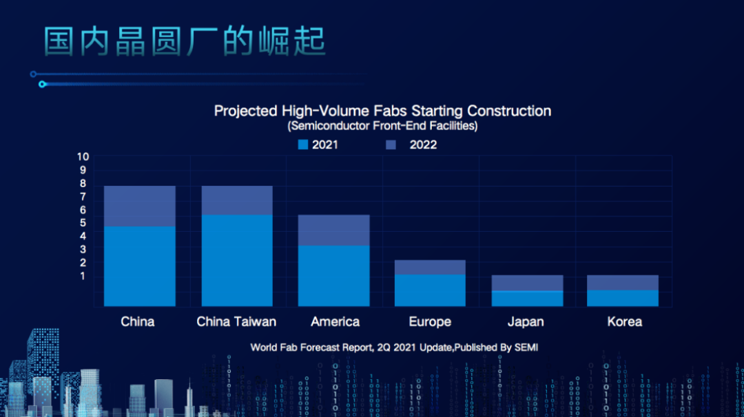
The number of domestic fabs is growing rapidly
According to SEMI data, mainland China's demand for semiconductor materials currently accounts for nearly 20% of global share, spanning various subcategories including photoresist, polishing slurry, and others. And the data shows this proportion has been steadily increasing since 2016.
Next, I'd like to share my personal perspective on some commonly used materials in semiconductor manufacturing and discuss their potential future directions.
First, substrate materials like silicon or gallium arsenide have a fairly clear evolution path — purity will keep increasing. Take silicon: 8-inch and smaller silicon wafers and silicon-based products require silicon purity of roughly seven or eight nines after the decimal point, known as 7N or 8N. But advanced silicon wafer processes and 12-inch wafers demand 11N or even 12N ultra-pure polysilicon. As chip sizes have grown from 4 inches to 12 inches, material precision requirements have risen accordingly.
Another emerging material trend in recent years, developing alongside new investment waves, is third-generation semiconductors such as silicon carbide and gallium nitride. Compared to conventional materials, these offer higher conductivity or greater durability — superior physical characteristics overall. This is one development trend we've observed on the materials side.
For materials like sputtering targets and specialty gases, the dimensions for improvement are relatively limited — essentially just increasing purity. Each process generation requires higher-purity products. These materials rarely see new product varieties during their evolution.
Turning to the ALD precursor field our company focuses on: ALD deposition offers better uniformity and step coverage compared to CVD and PVD deposition processes, making it more suitable for high-capacity memory manufacturing. And ALD precursors are the material foundation of this deposition process.
Beyond increasingly stringent purity requirements, precursor materials have two other critical evolution dimensions. First, process advances will drive demand for new varieties — for example, aluminum giving way to copper, or titanium being replaced by tantalum. This forces suppliers like us to operate like pharmaceutical R&D institutions, constantly developing new product types.
A brief aside: typically each new product type qualifies for 20 years of patent protection, which safeguards substantial profits during that period. However, China's current ALD precursor R&D remains in a catch-up position internationally. Most materials that have achieved domestic mass production may already be past their patent protection periods. This is the current industry reality.
The other evolution direction relates to a widely acknowledged bottleneck in ALD development. One shortcoming of ALD deposition technology is its relatively slow growth rate. Compared to other thin-film preparation techniques, ALD's advantages are clear — better film adhesion, better compositional uniformity — which has gradually made it a mainstream thin-film method. But research has found that current ALD technology typically achieves only about 15%-50% deposition of a single atomic layer per cycle, far below theoretical expectations. How to increase ALD deposition growth rates? This requires material suppliers and equipment makers to solve together.
04 Where Do Semiconductor Materials Companies Go Next?
As a materials company, we often get asked this question — we started in a niche market segment, but what if that segment eventually hits a development ceiling? Where do companies like ours go next? Let's look at the development paths of leading semiconductor materials companies.
Take JSR, the leader in photoresist. Originally a Japanese public-private joint venture, it started in synthetic rubber and synthetic resins, then leveraged its polymer R&D capabilities as a platform to expand into photoresist materials — since photoresist is fundamentally a polymer product as well. So its path was expanding through a polymer platform.
JSR official website
Companies in the sputtering target space are fundamentally working with metals, and their evolution direction is mainly about continuously improving metal purity. Nippon Mining & Metals, for example, started in specialty steel, then moved into electroplating materials based on its specialty steel smelting expertise, and later into targets — still essentially revolving around metal purification.
Merck Group's semiconductor division started with R&D processes for liquid crystal materials, then expanded to OLED materials, and then to ALD precursor materials. I see Merck's logic as using small-molecule chemistry as an R&D platform to expand within the semiconductor materials industry.
Shin-Etsu Chemical, by contrast, doesn't have such an obvious platform characteristic. It started mainly with silicon wafer substrates, then later moved into photoresist. I see it as using the semiconductor industry chain itself as its expansion method — first establishing a position within the semiconductor industry, then leveraging supply chain advantages to gradually extend into other upstream raw materials.
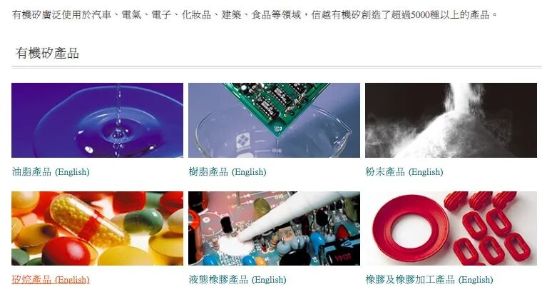
Shin-Etsu Chemical official website product display | ShinetsuOfficial
So how might semiconductor materials R&D evolve? This is a question I'm particularly eager to explore with all of you. Over roughly the past decade, we've observed quite a few successful R&D breakthroughs in the pharmaceutical sector. AI-driven drug discovery, for instance, has begun delivering meaningful assistance in new drug development. Take the small-molecule drug R&D process: researchers first need to select and identify which protein or nucleic acid serves as the drug's target, then design or synthesize lead compounds based on the target's spatial structure, and finally screen for the optimal candidate to advance into clinical development. AI can substantially boost efficiency at every stage of this process.
Could we apply similar logic to accelerate semiconductor materials R&D? In my view, our computational tools have already achieved the capability to simulate individual molecular materials — including OLED emitter molecules and the ALD precursor materials our company focuses on. If any of you or your investor networks have relevant resources, we'd welcome deeper discussions about whether such opportunities exist in this industry.
From what I've observed so far, there isn't yet a viable computational simulation approach that can genuinely assist materials R&D. Take photoresist, for example: we'd want to simulate the changes photoresist molecules undergo during processing — what happens when they absorb light, whether cross-linking can occur, and after cross-linking occurs, whether the boundaries remain clean during resist stripping with developer solution. These process-related aspects currently lack robust computational simulation. This may represent a future technological direction, but we believe it presents extraordinarily difficult challenges.
Finally, let me share what our company is working on. As mentioned earlier, our near-term goal is to achieve domestic production of ALD precursor materials needed upstream in wafer manufacturing — materials that currently have no domestic supply source and count among the critical "chokepoint" materials. Longer-term, as a materials company, we're thinking about how to grow beyond our initial niche market. We believe we can build a platform centered on high-purity organometallic compound R&D and production capabilities, gradually expanding into displays and new energy — such as lithium batteries and photovoltaics, which employ materials quite similar to ALD precursors, as well as catalysis methods and other areas.
Let me briefly introduce the ALD deposition technology our company specializes in. I like to use an analogy: ALD deposition is much like using transparent tape to pick up sand. No matter how much sand you pile onto the tape, it can only adhere in a single layer. If you want more sand on that layer of tape, you apply another coat of adhesive, and you can pick up another layer of sand.
ALD deposition works very similarly, except it deposits materials as single-atom-thin films, layer by layer, onto a substrate surface. First, the first precursor is introduced; after it saturates and adsorbs onto the substrate, excess reactants and byproducts are purged with inert gas. Then the second co-reactant is introduced, which reacts with the saturated first layer on the substrate surface. Excess molecules are purged again, and this cycle repeats — the atomic film on the substrate grows thicker, just like the accumulating sand.
One major advantage of this technology: because the chemical reaction between precursor and co-reactant is self-limiting, regardless of how complex the substrate surface is or how deep its trenches run, films deposited via ALD maintain highly uniform thickness and excellent conformality. This characteristic is critically important because as semiconductor technology advances, wafer surfaces have grown increasingly complex. For instance, the NAND flash memory architecture used in our phones and computer hard drives features extremely high aspect-ratio holes, with additional slots carved into the hole sidewalls. In such structures, achieving uniform thin-film deposition is only possible using ALD technology. Many memory architectures also contain large aspect-ratio structures requiring ALD-based film deposition.
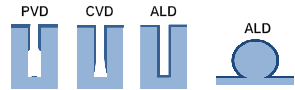
ALD thin-film deposition effect demonstration
Beyond this, our company is actively advancing ALD technology applications across different fields, with full confidence and determination.
These are my personal reflections on domestic semiconductor materials and an update on Origin Technologies' business progress that I'd like to share with you today. If you're interested, I'd welcome further discussion. Thank you.

▲Why We're Bullish on the Optical Chip Industry | FreeS Chip Series
▲Feng Li Column | A 2 Trillion Market and 10 Trillion Output: Why We're Bullish on China's Chips?
▲How Can Tech Companies Go from "Valuable Technology" to "Profitable Technology"? | FreeS Fund
▲FreeS 2021 Outlook ④ | Endgame Speculation on Sensors Behind Autonomous Driving