From Lithography to Nanoimprint: Challenges and Opportunities at the Semiconductor Industry's Turning Point | FreeS Fund Dialogue

After two decades on the sidelines, nanoimprint lithography is finally seeing the light of industrialization.

In mid-October, Canon announced the launch of its FPA-1200NZ2C nanoimprint lithography (NIL) semiconductor manufacturing equipment, capable of producing 5nm chips. According to Canon CEO Fujio Mitarai, the device will be priced "one digit less than ASML's EUV lithography machines." EUV stands for Extreme Ultraviolet Lithography, a photolithography technology using extreme ultraviolet wavelengths currently employed for advanced process nodes below 7 nanometers.
Prior to this, ASML was virtually the only company in the world capable of manufacturing EUV lithography machines. Giants like Nikon and Canon remained stuck at DUV (Deep Ultraviolet Lithography) machines — deep ultraviolet photolithography used for producing chips at the 7nm to 130nm process nodes.
The "rivalry" between nanoimprint lithography and photolithography has a long history. NIL is a micro- and nano-fabrication technology based on polymer embossing; to put it vividly, it's analogous to movable-type printing. Currently, NIL is widely used in LEDs, AR, and VR. Having developed for over two decades, NIL offers advantages over photolithography in terms of lower cost, simpler processes, and greater environmental friendliness. However, for a considerable period, because NIL-produced goods suffered from high defect rates and low yields, the semiconductor field was reluctant to adopt it — while photolithography advanced faster and performed better.
In the past decade, as NIL's process optimization and control precision have reached new levels, the technology — once dismissed by photolithography — has had its moment in the spotlight. Especially given the current context where China faces U.S. restrictions on exported photolithography equipment, NIL offers the possibility of leapfrogging for China's — and indeed the world's — semiconductor industry.
Focusing on this hot topic of nanoimprint lithography, we invited Professor Haixiong Ge, founder of Pulin Technology; Mengmeng Deng, co-founder and CEO of Pulin Technology; and Qianhang Yan, vice president at FreeS Fund, to discuss NIL's past, present, and future opportunities.

Topics they covered include, but are not limited to:
- What is nanoimprint lithography? Why is it suddenly trending?
- What are NIL's application scenarios?
- Compared to photolithography, what are NIL's advantages and disadvantages?
- As NIL enters the semiconductor field, which technical hurdles have been solved and which remain?
- Which domains can NIL help China "leapfrog" ahead in?
We've edited portions of their discussion into this article, hoping to offer fresh perspectives. We welcome you to continue observing and exploring with us. You're also invited to search for and subscribe to "Gao Neng Liang" on Xiaoyuzhou or Apple Podcasts to listen to the full episode.
Engagement Giveaway: What do you think about China's chip market? Where might China have opportunities to leapfrog ahead? Share your thoughts in the comments.
Until 17:00 on December 13, the 5 readers with the most thoughtful comments will receive Chip War, written by strategic consulting expert Sheng Yu. This book recounts the history of the global semiconductor industry from the perspective of corporate competition and national power.


**/ 01 / ** What Is Nanoimprint Lithography?
Why Is It Suddenly Trending?
Qianhang Yan: Recently, Canon announced it would launch NIL equipment comparable to DUV lithography machines and apply it to semiconductor processing. What exactly is this technology? Is it a replacement for photolithography, or a competitor?

▲ Canon's nanoimprint lithography equipment. Image source: Canon Global official website
Haixiong Ge: Nanoimprint lithography is a technology that emerged in the mid-1990s. At that time, photolithography — then in its heyday — had hit a bottleneck at the 100nm resolution mark. The industry hoped alternative technologies could push the semiconductor industry toward more advanced processes with higher resolution. Of course, today photolithography has made tremendous progress, achieving resolutions of 5nm and even 3nm.
What is nanoimprint lithography? There's a saying in the industry that Bi Sheng, the inventor of movable-type printing in ancient China, was the "progenitor of NIL." NIL is a micro- and nano-fabrication technology based on polymer embossing. It requires a template — just as a movable-type template has characters carved into it, an NIL template contains the nanostructures to be fabricated. Through heating and pressing, the nanostructures on the template are replicated into the NIL material.
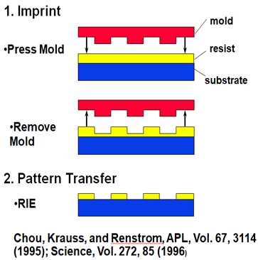
▲ Nanoimprint lithography steps. Source: Science
Qianhang Yan: Your analogy to movable-type printing is helpful — I'll offer another one: modeling clay. You take a mold, press it into a soft material like clay, then bake it. The clay hardens, and the pattern transfers from the mold to the clay.
Haixiong Ge: Or think of how we make mooncakes using a mold. You put the mooncake dough into the mold, and the finished mooncake comes out with the corresponding pattern.
Qianhang Yan: Breaking down the term "nanoimprint lithography," the "nano" part describes that it operates at the nanoscale, while "imprint" — like the mooncake and modeling clay examples — refers to the same technique or method of pattern realization.
Haixiong Ge: Since it's called "imprint," it is related to movable-type printing. Photolithography creates nanostructures through exposure; NIL creates them through printing.
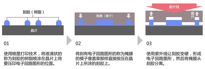
▲ Characteristics of nanoimprint lithography. Image source: Canon Club official website
Qianhang Yan: Before Canon's NIL announcement, there was speculation that Canon might enter the photolithography space. In recent years, DUV and EUV lithography machines have dominated the market conversation. After more than 20 years of development, why is NIL suddenly trending now?
Ge Haixiong: Nanoimprint lithography grabbed attention from the start because of its high resolution. Many people saw it as potentially a revolutionary micro- and nanofabrication technology. But NIL also has weaknesses — it's a physical contact-based process. During physical contact, external defects can easily occur. And the semiconductor industry has extremely low tolerance for defects. Some in the industry see NIL as very promising; others believe its defect rate is too high for semiconductor processing.
After falling behind ASML in conventional photolithography, Canon had been searching for new breakthroughs in semiconductor manufacturing — and found NIL. From recent reports, Canon's NIL technical specifications have matched DUV lithography in several areas, with some metrics even reaching EUV levels.
The concept of nanoimprint lithography was first proposed by my advisor, Professor Stephen Chou. Two or three years after Professor Chou introduced the concept, Professor C.G. Wilson at the University of Texas at Austin proposed the step-and-imprint approach. Professor Wilson, the main inventor of chemically amplified photoresists, had deep expertise in lithography technology and resist materials. He combined the step-and-repeat technique from photolithography with nanoimprinting, using UV-curable resin instead of thermoplastic polymers, and using UV exposure after imprinting to replicate patterns. Because UV exposure takes extremely little time — roughly a millisecond — it's well-suited for semiconductor processing.
Although NIL wasn't initially accepted by semiconductor manufacturing, it has already demonstrated strong application potential in non-semiconductor fields. For example, patterned sapphire substrates, a key component in LEDs, were originally made with photolithography. Thanks to NIL's simpler process, faster speed, and lower cost, replacing photolithography for patterned sapphire manufacturing looks very promising. Additionally, in optical devices like microlens arrays and blazed gratings, NIL has already shown manufacturing potential.
From our perspective, NIL has recently heated up again. In fact, before Canon's NIL announcement, the technology already gained significant attention in 2018, when AR and VR fields needed waveguide products — and NIL was an excellent choice for making them. Meanwhile, domestic demand for emerging technologies has felt stronger than in some European and American countries in recent years. So after seeing the prospects for AR and VR, many domestic companies turned their attention to NIL.
**/ 02 / ** **NIL Enters the Semiconductor Space: ** **Which Technical Hurdles Have Been Cleared, ** Which Remain Roadblocks? ** ** Qianhang Yan: Looking at the current landscape, what impact will Canon's focused NIL push have on upstream equipment suppliers in the semiconductor industry? Will its new moves and announcements bring fresh changes to the market?
Ge Haixiong: First, based on the technical parameters and metrics Canon has provided, NIL could potentially create some beneficial supplementation for the semiconductor field. ASML and Nikon's semiconductor lithography equipment is already widely adopted on production lines, so NIL can be seen as an extension of lithography technology.
But as we mentioned earlier, photolithography is a non-contact exposure process, while NIL is a physical contact-based preparation process. It will still take time for semiconductor manufacturers to adopt it. If Canon's new equipment truly has manufacturing capability and can demonstrate advantages like low cost, low energy consumption, and environmental friendliness, then semiconductor manufacturers might move toward broader acceptance.
Qianhang Yan: So from an industry acceptance standpoint, Canon's new move still needs a validation period?
Ge Haixiong: Yes.
Qianhang Yan: Professor Ge has spent over 20 years on NIL technology, equipment, and process R&D. Looking back, compared to when it was first invented, which technical challenges has NIL solved well, and which remain unresolved — becoming roadblocks to entering semiconductors?
Ge Haixiong: In 2001, I joined Professor Stephen Chou's group — the inventor of NIL — as a postdoc. My background was in polymer materials; Professor Chou's was in microelectronics and micro/nanofabrication. Because NIL materials could be directly compared to photoresist materials, I went there to develop NIL materials.
At that time, Professor Wilson had just proposed the step-and-imprint nanoimprint concept. He used UV curing to solve the problem of long processing times in thermal nanoimprinting, dramatically improving NIL throughput.
Later, Professor Wilson founded Molecular Imprints to continue step-and-imprint NIL R&D. This company attracted investment from Canon. In 2014, Canon directly acquired Molecular Imprints' semiconductor NIL division, helping Canon specifically develop NIL technology.
Early NIL technology wasn't accepted by some semiconductor peers due to high defect rates and low yields. But after acquiring Molecular Imprints, Canon applied many semiconductor manufacturing techniques to NIL. For example, in semiconductor production, cleanroom cleanliness is generally Class 0 — meaning essentially no particles — and Canon brought NIL environments to Class 0 levels as well, further pushing NIL applications in semiconductors.
Another reason some believed NIL wasn't suitable for semiconductor processing was the alignment requirement in semiconductor manufacturing. NIL is a mechanical imprinting process, and people worried that imprinting slippage would degrade overlay precision.
Specifically, when we make transistors, a chip doesn't have just one layer — it might have dozens or hundreds of transistor layers. Each time we fabricate, we need to process transistors on top of the previous layer, at scales of 10 nanometers or a dozen-plus nanometers. We call this lithographic overlay, requiring alignment precision approaching 1-2 nanometers.
Canon itself manufactures lithography equipment and has a complete alignment technology pathway, so it applied existing lithography alignment techniques to NIL. Current NIL actually combines nanoimprint concepts with lithography technology — "nanoimprint lithography" would be more accurate.
From Canon's published technical specifications, its current alignment precision is approaching 1 nanometer, meeting the requirements for preparing transistor structures at the dozen-nanometer or few-nanometer scales previously done by DUV and EUV.
Templates are also a constraint on NIL. When photolithography masks are exposed, optical systems can shrink 100-nanometer scales down to 20 nanometers. But NIL has no reduction process — whatever resolution the nanostructures on the template have, that's the resolution replicated in the imprint resist.
Qianhang Yan: If you want to further improve template precision, how would you do it? Or is this like Moore's Law, where eventually there's a ceiling on how far process nodes can advance?
Ge Haixiong: It's generally accepted that NIL templates can also be made with lithography technology. Some might say: if templates still need DUV or EUV, what advantage does NIL have?
NIL is a high-fidelity replication process — that's its technical advantage. Once you make one template with DUV or EUV, NIL can use that template to further replicate more daughter templates, granddaughter templates. Also, like photolithography masks, NIL templates can be made with electron beam lithography.
To add: we've recently seen the National Natural Science Foundation exploring whether semiconductor devices still follow Moore-era patterns after Moore's Law失效. NIL is also considered potentially applicable for manufacturing devices at 1 nanometer or sub-nanometer scales. The foundation's programs have also raised questions about how to perform anti-sticking, anti-adhesion treatment on templates at sub-nanometer scales. These issues remain to be further explored.
Compared to Lithography, What Are NIL's Advantages and Disadvantages?
Qianhang Yan: In fields like patterned substrates and optical devices, NIL has replaced lithography as the mainstream technology. Setting aside specific implementation difficulties and looking at the technology itself, what are the relative advantages and disadvantages of NIL and lithography? Why have some industries originally using lithography now chosen NIL?
Ge Haixiong: Photolithography is generally considered to have descended from photography, which has developed for nearly two centuries. Lithography itself began developing in the 1950s and, over seven or eight decades, has become extremely mature — even reaching an极致境界. This is lithography's advantage.
Compared to lithography, NIL has a shorter development history. It emerged in 1995. NIL's advantages lie in high resolution, simple replication process, and low cost.
First, resolution. Early NIL achieved resolution below 10 nanometers, far exceeding lithography's resolution at the time, attracting significant attention. After more than 20 years of development, NIL's minimum resolution can reach roughly 1 nanometer. We generally use dense line grating structures to benchmark NIL against lithography. Currently, lithography can only achieve dense line gratings above 10 nanometers, while NIL can now achieve 8-nanometer period, 4-nanometer line width dense line grating structures. So NIL maintains its resolution advantage.
Second, replication process complexity. NIL can directly replicate needed nanostructures or microstructures into functional materials — optical materials, catalytic materials, even the currently hot perovskite materials. This capability lithography doesn't have. Lithography always replicates into photoresist materials, which typically only serve lithographic functions without integrating other application functionalities.
NIL produces 3D-structured patterns, which lithography cannot do. Meanwhile, lens structures, microlens arrays, AR/VR waveguide blazed gratings, and high-resolution, high-steepness, high-aspect-ratio gratings can all be processed in one step through NIL.
Finally, cost. NIL is low-cost because once structures are made on the template, they can be imprinted into NIL resist. In lithography, needed patterns are exposed into photoresist through exposure, and both DUV and EUV lithography use high-energy light sources that consume enormous energy during processing. NIL only requires simple UV exposure, needing far less energy than lithography.
From current reports related to Canon, if NIL is used to produce chips around 10 nanometers, NIL technology costs roughly one-third of DUV or EUV. For products like patterned sapphire substrates and gratings, NIL's cost advantage may be even greater.
Deng Mengmeng: NIL currently has another advantage in LED chip manufacturing: lithography requires a development step, while NIL doesn't. After UV curing, the entire 3D pattern forms. At this stage, NIL saves additional investment and process costs. In the LED chip manufacturing industry, stepper lithography costs under 4 yuan to process one wafer, while NIL can achieve 1.5 yuan per wafer — a clear cost advantage.
Which Domestic Fields Can NIL Help Achieve Leapfrog Development?
Qianhang Yan: Nowadays, quite a few advanced domestic process tools are under embargo. From the NIL perspective, I'd like to ask Professor Ge and Ms. Deng to talk about which domestic fields could achieve leapfrog development through NIL.
Ge Haixiong: Due to certain external technology blockades, it's difficult for us to directly access lithography technology, so the industry is hoping for new technologies that can replace it. From a technical standpoint, NIL is far less complex than lithography because it lacks the complex exposure system, while lithography's alignment and overlay techniques can be adapted to NIL. Although NIL still has hurdles to overcome for true semiconductor applications, there are fewer barriers compared to lithography, making it more likely to achieve a technological path change.
Deng Mengmeng: As we mentioned earlier, one of NIL's advantages is its extremely low cost — production efficiency is several times that of current lithography. We've learned that 16 NIL machines can produce over 10 million wafers annually, with per-wafer costs dropping to 1/2 to 1/3 of lithography.
Actually, NIL isn't just for semiconductors. Its applications target three major industries: first, display and consumer electronics; second, automotive; and third, biomedical.
Especially in consumer electronics, NIL has now replaced most lithography-based manufacturing solutions and production lines. The reason is that it doesn't require subsequent etching processes, so it essentially completes micro-nano structure fabrication directly. The entire industry is increasingly favoring NIL.
From an optical perspective, NIL has another advantage: it can directly shape functional materials — whether high-refractive-index materials, low-refractive-index materials, or materials with special functions — into the micro-nano structures desired for the target product. For example, new imaging devices made with NIL can reduce the thickness of smartphone camera modules from four or three lens elements down to one.
In a sense, as micro-nano optical technology develops, it will completely surpass the performance advantages of traditional convex-concave lenses. This is something optical manufacturers are quite certain about — micro-nano optics will replace geometric optics, while costs will be much lower than DUV or EUV.
In the biomedical field, many detection technologies, especially fifth-generation gene sequencing, use micro-nano structures. Currently some of this is done with DUV lithography, but its relatively high cost means there's a desire to reduce expenses in later-stage testing.
NIL actually has quite broad applications and relatively high market acceptance. From a perspective other than cost, people might prefer lithography. But I believe as the industry develops and matures, the ultimate goal is to optimize production costs and processes to the extreme, rather than relying on just one technology to finally reduce costs, produce products, and achieve end goals.
Ge Haixiong: Actually, in some fields, lithography has no competitive advantage over NIL. Because lithography simply can't be applied in many areas — for example, microlens arrays, and AR/VR gratings have refractive index requirements, while lithography uses photoresist, which generally can't serve directly as a functional material.
Qianhang Yan: We just mentioned quite a few fields where NIL can replace lithography processes. What common characteristics do these fields share that drives NIL adoption?
Deng Mengmeng: Imprint replacing lithography is really more about semiconductor process flows, especially in industries with etching processes. Because if you're simply doing material shaping on some product surfaces, lithography isn't the optimal technical choice — imprinting better demonstrates advantages like low cost, simple processes, and mass production capability. In optical applications, consumer electronics, automotive, biomedical, and new energy fields, the industry may prefer one-step forming as the optimal solution.
Ge Haixiong: From the micro-nano structure perspective, if you need one-step forming of 3D structures with certain complex morphologies, then NIL has unique advantages. Additionally, for some high-density array structures, NIL is also very advantageous.
Qianhang Yan: For many domestic industry customers, NIL may be an entirely new technology. In promoting NIL, what are customers' views and attitudes? Which types of customers have shown unexpectedly strong interest in NIL?
Deng Mengmeng: Currently in the domestic market, many industries — especially in optics — are very actively advancing imprint-related process routes in micro-nano optical manufacturing, R&D. Some leading lithography companies are also actively pushing NIL-related technical routes.
Beyond optics, several of the largest domestic display panel manufacturers are in communication with us. They now not only have 8-inch and 12-inch wafer-type samples and products, but have also proposed manufacturing solutions for large-format NIL products at 1 meter by 1.2 meters.
The industry that surprised us is actually new energy, especially perovskites. We didn't expect imprinting to have such large application scenarios in this industry. The perovskite principle is similar to LED — patterning materials to enhance certain optical properties in the material, thereby improving photoelectric conversion efficiency. We also have related applications and products being used by foreign customers.
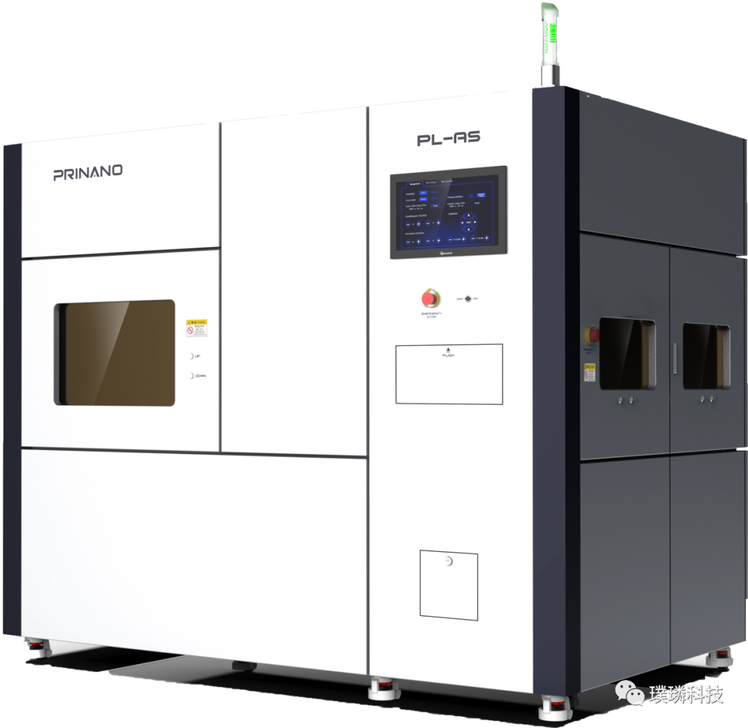
▲ Wafer-level semiconductor nanoimprint system. Source: Pulin Technology
Qianhang Yan: If you were to summarize the industry's overall attitude and views toward NIL, what stage is everyone at? Are they in a new technology exploration and experimentation phase? Or are there individual industries that have already firmly chosen NIL?
Deng Mengmeng: The industry where NIL has entered most quickly is LED. Facing technology blockades, one domestic LED manufacturing company adopted NIL technology and gained tremendous advantages, prompting the entire industry to relatively quickly move toward a direction led by NIL.
Today, NIL has numerous application scenarios in optics, drones, automotive, biomedical — especially in gene testing. This was hard to imagine last year and even earlier this year.
From a macro perspective, all enterprises previously related to micro-nano manufacturing have more or less shifted their attitudes toward NIL — from not understanding it, to watching and waiting, to being willing to use imprint technology for innovation and new R&D.
We believe this is a pre-burst state for the industry. If given more time and development space, new applications of NIL in the new energy track will become increasingly numerous and broad.
After 20 Years in the Cold, the Dawn of Industrialization
Qianhang Yan: Professor Ge spent the past 20 years as an academic, and started his company in 2017. What experiences can you share with other domestic scholars looking to commercialize their research?
Ge Haixiong: First, I want to thank FreeS Fund for their timely investment. After FreeS's investment, we could clearly feel NIL attracting increasing attention from various industries — including the market demand for AR and VR that emerged this year, and Canon's recent introduction of new NIL technology.
We were originally doing research. First, we needed to make the technology feasible for落地 and commercialization. We need to "reach for the sky while standing on the ground" — doing cutting-edge research while making the end goal serve daily life, or serve our technological progress and production. In the technology落地 process, we also need to constantly challenge ourselves, continuously advance technological progress, so that technology can match market demands and continuously satisfy industrial application needs.
Qianhang Yan: From a competition or entrepreneurship perspective, what characteristics and advantages does Pulin Technology have that enable it to stand at the风口 of NIL entering semiconductors, and continuously advance NIL technology落地 and commercialization across various scenarios and fields in China?
Ge Haixiong: We often say that NIL, like lithography, is a technology requiring craftsmanship. We've been deeply engaged in NIL for over 20 years. Because I had the opportunity to study the most advanced NIL technology in the team of NIL's inventor, I know NIL's advantages, shortcomings, and directions needing development. Additionally, my materials background is key — materials are a critical part of NIL technology, so we also understand NIL processes very well. We know how to match process materials with our equipment, and develop equipment suited to NIL's technical characteristics.
Qianhang Yan: Currently in the NIL direction, what R&D has Pulin Technology done? For NIL's domestic semiconductor push, how does Pulin plan to contribute to this major trend?
Deng Mengmeng: As Professor Ge said, whether making a product with lithography or imprint technology, you first need to clear the entire process route — including what materials to use, what imprint method to use.
Pulin Technology's technical routes and reserves all come from Nanjing University's NIL Application Laboratory. Currently Pulin has developed not only etching-type NIL materials for semiconductor manufacturing, but also functional materials now widely used in the optical market, and other functional materials for biomedical applications. Some of these are already in full mass production and shipped to our downstream customers.
For different application scenarios, we also have different NIL equipment — especially for semiconductor manufacturing, we have step-and-repeat NIL equipment. At the same time, we're also researching how to reduce step-and-repeat imprint alignment precision to below 100 nanometers.
Ge Haixiong: In the early stage, we did verification of NIL technology applications in semiconductor manufacturing — such as etching transfer processes, minimum resolution, and pattern fidelity verification. We also did verification using imprint alignment processes.
Qianhang Yan: Finally, let's imagine the future. When NIL technology was born, it was an alternative technology competing with lithography. After 20 years in the cold, NIL now faces the dawn of industrialization. What will the mutual relationship between lithography and NIL technologies be in the future? What will their positions be in the industry?
Ge Haixiong: Lithography technology is very mature, while NIL is still in its infancy. In the short term, NIL is unlikely to fully replace lithography. Of course, NIL can serve as a beneficial complement to lithography. In some fields, it can first develop and break through, then possibly gradually mature and do more.
NIL's development requires joint efforts and coordination across the industrial chain. Because lithography's development satisfied the application needs of large enterprises like Intel, TSMC, and Samsung, and their use of lithography also drove its advancement. We need more enterprises to accept this emerging NIL technology and integrate it into production and manufacturing, continuously improving.
Additionally, enterprises applying NIL need more talent familiar with and mastering NIL technology. Currently some mass-production equipment is not mature enough, constraining NIL's applications in many fields. We hope enterprises in the industrial chain can cooperate with NIL research companies like ours to jointly develop equipment suitable for NIL scenarios.
Reader Giveaway
What do you think about China's chip market? What leapfrog opportunities might China have? Share your thoughts in the comments.
By 17:00 on December 13, the 5 readers with the most thoughtful comments will receive Chip War, written by strategic consulting expert Yu Sheng. This book tells the history of global chip industry development from the perspective of corporate competition and national power rivalry.

Amid the GPT Frenzy: Anxiety and Breakthroughs in China's Chip Market | FreeS Fund
What Happens When the Hottest Tech Tracks Converge? | FreeS Chip Series
Was Elon Musk Right? Will LiDAR Make It Into Cars? | FreeS Chip Series
Star the FreeS Fund WeChat Official Account — timely business insights delivered straight to you