Adaps Photonics has released China's first dToF sensor built with 3D stacking technology, offering a groundbreaking solution for 3D sensing.

Overall performance reaches world-class standards.
On July 13, Adaps Photonics (hereinafter referred to as "Adaps") announced the release of its self-developed ADS3003 dToF single-photon imaging sensor (SPAD image sensor, SPADIS), which uses globally advanced backside-illuminated 3D stacking process technology. The sensor's overall performance reaches world-class standards, providing a groundbreaking solution for high-end consumer electronics, LiDAR, and other 3D perception applications.
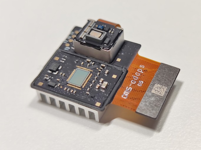
A dToF 3D imaging module equipped with the Adaps ADS3003, jointly developed by Adaps and Omnivision Electronics.
Founded in May 2018 by four PhD returnees from prestigious universities, Adaps is dedicated to providing self-developed, high-performance dToF depth sensor chips using internationally leading single-photon detector (SPAD) technology for applications in smartphones, LiDAR, robotics, VR/AR devices, and more. Gaorong Ventures invested in Adaps in 2021.
3D sensing technology is expanding into cutting-edge application areas such as consumer electronics, automotive electronics, and industrial control. Among these, direct time of flight (dToF) technology represents the forefront of 3D sensing — it obtains target distance by detecting the flight time (round-trip) of light pulses, thereby achieving 3D imaging of objects. With its superior ranging capability, power efficiency, and anti-interference performance, this technology has garnered increasing attention from industry in recent years. Particularly after Apple released its dToF imaging solution (LiDAR Scanner) for mobile ecosystems in 2020, and Sony unveiled its dToF-based automotive LiDAR solution, market demand for advanced dToF imaging chips has exploded.
The ADS3003 dToF single-photon imaging sensor released by Adaps features a physical resolution of 240×160, a 0.35-inch array size, and employs backside-illuminated 3D stacking process technology. It achieves measurement distances of up to 15 meters indoors and 5 meters outdoors, with a maximum frame rate of 50fps. It enables full-range sub-centimeter ranging accuracy and depth resolution, fully meeting demands ranging from smartphones and AR devices to robot vacuums, smart home IoT, and industrial measurement applications. Adaps has also simultaneously launched a dToF module solution based on this chip in partnership with Omnivision Electronics.
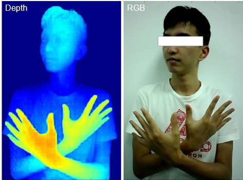
Left: Human imaging captured by the Adaps ADS3003; Right: RGB imaging of the same scene. The ADS3003 demonstrates excellent sensing quality for faces and hand gestures, with superior detail capture for low-reflectivity objects such as hair.
Furthermore, the Adaps ADS3003 is China's first dToF sensing chip to employ 3D stacking technology. To date, fewer than five companies worldwide are known to have released 3D-stacked dToF chip products. 3D stacking technology allows the photon detector (SPAD) portion and the logic circuit portion of the sensor chip to be processed on separate wafers, then merged into a single complete chip through hybrid metal bonding. This design enables the chip to obtain greater circuit area without increasing its footprint, allows the photon detector and logic circuits to each use the most suitable process node, and achieves higher SPAD photon detection efficiency (PDE), higher resolution, lower power consumption, and better overall performance. Previously, this process technology was only seen in the LiDAR Scanner chip jointly developed by Apple and Sony for iPad Pro and iPhone 12 Pro. The Adaps ADS3003 has surpassed that chip in both resolution and ranging capability.
"Comparing against the cutting edge of international dToF sensing, we found that 3D stacking technology is the key to achieving high performance, large resolution, and low power consumption — it is a prerequisite for fully unlocking dToF sensing potential," said Kai Zang, CEO of Adaps Photonics. "Adaps has invested over two years in 3D stacking technology R&D. We are one of very few companies globally, and the only one domestically, capable of providing mature, high-performance dToF chips and complete solutions based on backside-illuminated 3D stacking process. We see increasingly clear demand for 3D perception across more industries and products. Through this product, Adaps hopes to leverage our advantages to help our customers truly make the leap from 2D imaging to 3D perception."
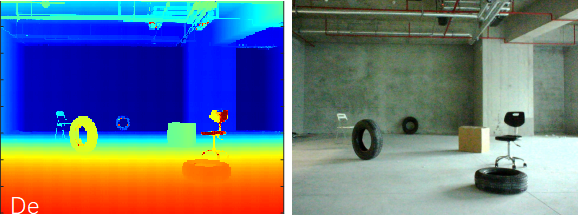
Left: Long-distance indoor scene imaging by the Adaps ADS3003; Right: RGB imaging of the same scene. The farthest tire is 13 meters from the sensor, yet its outline remains clearly visible. This demonstrates the ADS3003's excellent ranging capability for low-reflectivity objects while maintaining low power consumption and a wide field of view.
The Adaps ADS3003 chip will begin providing samples and test kits to customers in July 2021. The chip has already achieved preliminary mass production capability. Going forward, Adaps will continue to deepen its expertise in advanced dToF sensing technology, consistently providing market-leading 3D sensing chip products for the market and its customers.
Adaps Photonics will soon open applications for chip and evaluation kits based on Woodpecker. For details, please contact: lili.zhang@adaps-ph.com; ben.tian@adaps-ph.com


Kaikeba Secures 600 Million Yuan in Series B1 to Further Advance Online Vocational Education