Adaps Photonics Closes Series C2 Round to Accelerate R&D and Mass Production of High-End 3D Camera Chips

In 2023, it developed the world's highest-pixel SPAD array chip at the time.

On July 31, Adaps Photonics announced the completion of its Series C2 funding round, led by Jintou Dingxin, an investment arm of Zhejiang Financial Holdings. The proceeds will be used to accelerate R&D iteration and mass production of high-end 3D camera chips. Gaorong Ventures led Adaps Photonics' Series B1 round in 2021 and continued to increase its stake in the Series C round.
The company is committed to serving as a hardware enabler, empowering advanced 3D camera chips to drive technological capabilities in autonomous driving, robotics, and high-end imaging — making "unified sensing and computation for 2D and 3D imaging, flexible and generalized end-to-end intelligent perception, and extreme low-light high-frame-rate imaging" a reality. In the first half of 2024, Adaps Photonics saw rapid business growth, entering the supply chains of multiple Chinese industry leaders and achieving mass production and shipment of high-end chip projects.

Deep Expertise in SPAD Technology, Industry-Leading Products
Founded in May 2018 by several PhDs from Stanford University and Delft University of Technology, Adaps Photonics has a core team with years of deep experience in SPAD technology. The company possesses internationally leading full-stack SPAD device design and process capabilities, holds multiple independently developed SPAD patents domestically and abroad, and has been recognized by the Ministry of Industry and Information Technology as a national-level "Little Giant" specialized and innovative enterprise.
Adaps Photonics has launched products including SiPMs, single-photon imaging SPAD array chips, and multi-point and limited-point dToF chips and modules, continuously accelerating application deployment in smart vehicles, premium smartphones, robotics, automatic control, human-machine interaction, and smart home sectors.
Notably, the company successfully taped out its 3D-stacked SPAD array chip in 2021, and in 2023 developed the world's highest-pixel-count SPAD array chip, enabling solid-state 3D camera imaging. Its SiPM based on 905nm was the first to break the world record for PDE parameters, reaching 25%, and in 2023 received AEC-Q102 Grade 1 automotive certification — meeting the stringent performance and reliability standards for automotive LiDAR. By the end of 2023, it had achieved stable, scaled mass production and shipment. Multi-point and limited-point products have successively entered the supply chains of various leading manufacturers throughout the year, with continuous iteration and batch shipment.
Adaps Photonics' million-pixel-class array chip is expected to hit the market in the future. The company has substantial technical accumulation in array imaging chips, with a technology roadmap that leads industry, academia, and research institutions at home and abroad. In August 2023, Adaps Photonics released the ADS6311 chip, which led the industry's most cutting-edge large-format SPAD array product planning and parameter definitions at the time. The chip's photosensitive area features 768×576 SPADs, with every 3×3 SPADs forming one super-pixel, achieving a point cloud resolution of 256×192. The ADS6311 is also one of the highest-resolution pure solid-state LiDAR SPAD array chips currently on the market, widely applicable to automotive, robotics, and other pure solid-state LiDAR fields, and has secured design wins from numerous top-tier technology companies globally.
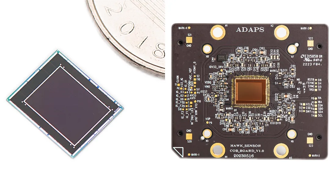
ADS6311 Chip and Development Board
Building 3D Sensing Chip R&D Capabilities
Expanding High-End Intelligent Application Scenarios
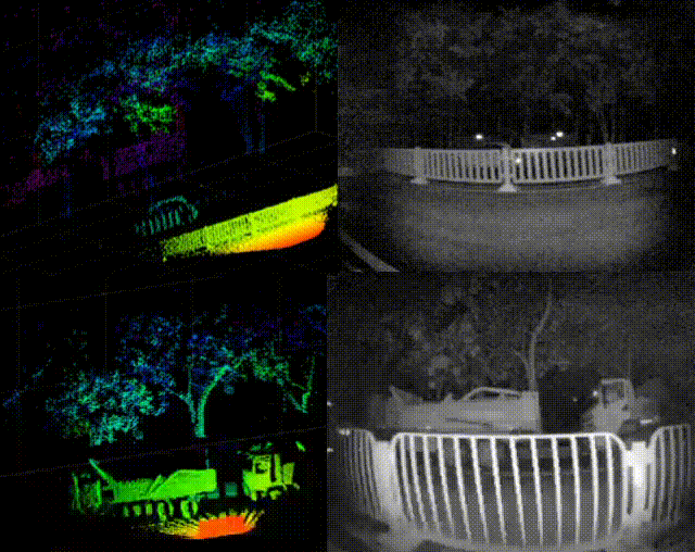
As the core component of pure solid-state 3D cameras, SPAD array sensor chips have strategic significance in defining the performance ceiling of complete systems. Future 3D cameras will only require 3D-stacked SPAD array chips, transmitters, and lenses — transforming LiDAR from a "precision instrument with moving parts" into a "3D camera device capable of mass production," thereby significantly reducing costs for autonomous driving LiDAR.
Meanwhile, as AGVs, AMRs, humanoid robots, and surveillance cameras evolve toward greater intelligence, connectivity, and interactivity, industry demands on sensors continue to rise, with industrial control and security customers increasingly preferring automotive-grade products. Adaps Photonics' automotive-grade certification and validation in the automotive market lay a solid foundation for expanding into industrial control and security applications.
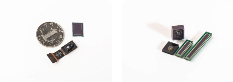
Consumer SPAD dToF Array & LiDAR Silicon Photomultiplier Products
Adaps Photonics stated that the company has continuously built its 3D sensing chip R&D capabilities, achieving rapid iteration toward higher pixel counts in SPAD array products through sustained multi-generation product planning, constantly strengthening its technical leadership. At the same time, the company has achieved effective integration of technology and market, accelerating scaled mass production for high-end intelligent application scenarios. "Step by step, winning from afar — going forward, Adaps Photonics will continue to lead market development as a pioneer in the high-end advancement of 3D SPAD array chips."