Adaps Photonics Closes Hundreds of Millions of RMB in Series C Funding, Global Leader in 3D Sensor Chip Technology

Deeply embedding itself in high-growth application markets such as smartphone 3D sensing, automotive LiDAR, and AR devices — building the "perceptive eyes" of the digital world.

Adaps Photonics, a next-generation global leader in 3D sensor chips, has completed a Series C financing round of several hundred million RMB. Meituan Longzhu led the round, with existing investors Kinzon Capital and Gaorong Ventures continuing to increase their stakes. Following this financing, the company will accelerate mass production of its products and continue investing in R&D for advanced applications to maintain its technological edge. Gaorong Ventures previously led Adaps Photonics' Series B1 round in 2021.

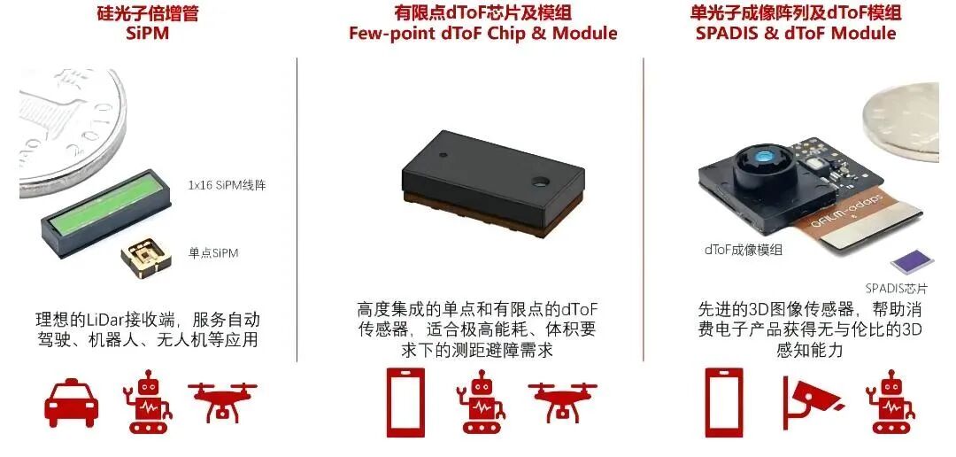
Independently developed high-performance dToF depth sensor chips, widely used in mobile phones, automobiles, industrial applications, and more
Adaps Photonics is dedicated to using internationally leading single-photon avalanche diode (SPAD) technology to provide independently developed high-performance dToF depth sensor chips for mobile phones, LiDAR, robots, AR devices, and other applications. Since its founding in 2018, Adaps Photonics has rapidly completed multiple financing rounds and attracted strategic investments from Xiaomi, OPPO, and OFILM.
dToF (direct time-of-flight) works by emitting light pulses directly at the measured object and calculating the distance based on the time interval between the emitted and reflected pulses. Depending on system perception requirements, dToF can perform single-point ranging or imaging in conjunction with scanning or optical lenses, making it widely applicable for depth sensing in mobile phones, automobiles, smart home devices, and industrial equipment.
In recent years, dToF has gradually become an industry focus and entered a period of rapid growth, driven by the inclusion of LiDAR in iPhone 12/13 Pro models and Sony's launch of stacked SPAD depth sensors for automotive LiDAR. According to projections, the dToF market will continue to grow rapidly over the next five years. By 2026, the dToF industry chain is expected to form a trillion-dollar market, with chip, module, and system markets potentially exceeding $20 billion, giving rise to new industry giants.
Internationally leading SPAD device design and process capabilities, with multiple 3D-stacked SPADIS chips successfully developed
Adaps Photonics focuses on dToF technology and possesses exceptionally high core technical barriers. The company masters internationally leading SPAD device design and process capabilities, achieving a photon detection efficiency (PDE) of 25% at the 905nm wavelength — a world-record level that far exceeds the industry average of 5%-18%, enabling longer detection range, lower power consumption, and smaller form factors. Adaps Photonics also possesses the only mature 3D-stacked dToF chip design and process capabilities in China, and among the rare few globally, having successfully developed multiple 3D-stacked SPADIS chips.
Currently, Adaps Photonics' independently developed single-photon imaging array (SPADIS) chips and dToF modules, silicon photomultipliers (SiPM), and limited-point dToF chips and modules have all met expected performance benchmarks in evaluations. Going forward, Adaps Photonics will comprehensively drive mass production of its dToF chip products to meet rapidly growing demand for advanced dToF products from customers in mobile phones, automotive LiDAR, robotics, and other sectors.
Deep cultivation of cutting-edge 3D sensing technology, building the "insightful eyes" of the digital world
Behind these high technical barriers and leading products stands a team of academic elites and seasoned semiconductor industry professionals. The company's core founding team holds PhDs from top overseas universities, with many years of experience in SPAD & dToF frontier research and multiple top-tier academic publications in related fields. Adaps Photonics also maintains a strategic advisory team composed of top industry technical experts.
In the view of Zang Kai, Chairman and CEO of Adaps Photonics, future digitalization will strengthen the connection between the virtual world, the digital world, and the physical world. 3D sensing technology is a crucial component of this — ranging, positioning, and modeling are all raising the bar for 3D sensing technology itself. As a cutting-edge 3D sensing technology, dToF, particularly 3D-stacked dToF, may become the "insightful eyes" of the digital world.
Going forward, Adaps Photonics will continue developing products with superior performance while deeply positioning itself in high-growth application markets including mobile 3D sensing, automotive radar, and AR devices, gradually growing into a domestic dToF leader and making its mark on the global dToF market.
Michael Mao, Founding Partner of Gaorong Ventures, stated: "The future digital world requires not only image information but also depth-based 3D information. The application market for 3D sensing technology is expanding rapidly, with surging demand in consumer electronics, automotive, and industrial robotics. Since our investment in Adaps Photonics, we have seen the team leverage its profound understanding of 3D vision market needs and its dedicated work in dToF technology to create world-class dToF chip products that meet market expectations. We look forward to Adaps Photonics achieving even greater progress in its upcoming journey toward mass production and commercialization."