A Conversation with Adaps Photonics: From LiDAR to Optical Communications, Becoming a Photonic Chip Player in the AI World | Gaorong Ventures

First "see the world," then understand it.
In the AI era, photonic chips — capable of emitting light, receiving light, and converting between optical and electrical signals — are increasingly taking center stage as core components for 3D perception, LiDAR, and optical communications.
Among these, SPAD chips are a type of photonic chip that receives optical signals and converts them into electrical signals. SPAD (Single Photon Avalanche Diode) is an ultrasensitive photodetector capable of detecting individual photons. Even in extremely dark environments, it can keenly capture faint light signals, earning it the nickname "photon catcher." In recent years, SPAD dToF chips have become widely known in the industry and among the public as core components of LiDAR.
Founded in 2018, Adaps Photonics is the undisputed leader in China's SPAD space. Adaps Photonics possesses internationally leading capabilities in SPAD device design and 3D stacking processes, making it one of the few companies globally to master core technologies and achieve stable mass production. In the automotive LiDAR market, Adaps Photonics is the only domestic manufacturer to have achieved mass production of automotive SPAD chips, with shipments continuing to lead the pack.
In 2026, building on its accumulated expertise in SPAD, Adaps Photonics is actively entering the optical communications field and is committed to becoming a photonic foundational technology platform company for the AI era.
Recently, we sat down with Kai Zang, founder and CEO of Adaps Photonics, to discuss how the company is building a full-scenario product matrix starting from SPAD as its core technology, and empowering key industries in the AI world. In his view, whether for robotics, autonomous driving, or AI data centers, "you need to see the world first, then understand it." Gaorong Ventures led Adaps Photonics' Series B1 round in 2021 and continued to invest in its Series C round.


The Adaps Photonics story began with Kai Zang's research on SPAD during his PhD at Stanford University. He noticed a cross-disciplinary research trend at the time — replicating biological features from nature onto nanoengineering. A typical application was scientists developing gecko-inspired nanofiber adhesive technology based on the microscopic structure and adhesion principles of gecko toes, which could be used for climbing robots, biomimetic climbing gloves, and other applications.
This inspired Kai Zang: Could SPAD technology enable intelligent machines to possess powerful 3D perception capabilities comparable to the human eye, accurately sensing the world in any environment?
"From a bionics perspective, the human eye has cone cells and rod cells. Cone cells are sensitive to color perception but weak in low-light recognition, similar to cameras; rod cells, which make up over 80% of the eye's neural cells, have two key characteristics — single-photon recognition capability and extremely fast response speed. That's why the human eye can clearly capture fleeting moments. SPAD possesses exactly this kind of ability."
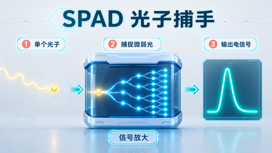
Of course, bionics inspired Kai Zang with more than just SPAD itself — it provided a methodology: "Find underlying mechanisms that have been long validated in nature, then use engineering to transform them into scalable platform capabilities." During his time at Stanford, beyond single-photon detection technology, Kai Zang also worked extensively on optical communications, micro-nano optics, biosensing, and other directions. These seemingly different fields all revolved around the same fundamental question — how to acquire, transmit, and process information.
Subsequently, during his PhD, Kai Zang successfully proposed an innovative "light-trapping structured single-photon detector" solution, laying the groundwork for SPAD monolithic integration and low-cost mass production. The research was published in the top-tier academic journal Nature Communications.
"I still remember when I graduated, the Apple iPhone LiDAR solution R&D team came to my thesis defense as a group. That made me realize this technology had the potential to be productized in the future."
After completing his PhD, Kai Zang joined Microsoft's HoloLens virtual reality product group, responsible for optical display and sensing work. There, he saw the opportunity to apply SPAD to AR/VR glasses, while also noticing teams like Google Self-Driving Car exploring SPAD chip applications. This further clarified for him the industrial prospects of this foundational technology.
In 2018, armed with firm confidence in the Chinese market, industrial chain foundation, and engineering capabilities, Kai Zang returned to China and founded Adaps Photonics, with SPAD technology as the entry point for his venture. However, rather than building around a single product, Kai Zang preferred to think in terms of underlying technology platforms — a "technology gene" that would later enable the company to continuously extend its business boundaries.

At its founding, Adaps Photonics targeted the consumer electronics market. Around 2021, as China's new energy vehicle penetration rate reached an inflection point, Kai Zang and his team judged that domestic substitution for core automotive components would become an irreversible industry trend. The company quickly pivoted to fully invest in automotive-grade LiDAR chip R&D, becoming the first domestic company to achieve complete supply chain localization for automotive-grade LiDAR SPAD chips.
In 2023, Adaps Photonics achieved large-scale mass production of automotive-grade SPAD dToF chips, fully integrating into the core intelligent driving supply chain.
As is well known, the intelligent driving industry has long debated pure vision versus LiDAR approaches — Tesla previously championed camera-based perception, arguing that cars don't need LiDAR. "I've always felt that pitting cameras against LiDAR is itself a false proposition," Kai Zang said. "Imagine when we're running at night, we instinctively slow down because our eyes can't accurately judge our surroundings as they do during the day. Yet bats can fly at high speeds in complete darkness because they use ultrasonic echolocation for ranging, obstacle avoidance, and hunting. For intelligent driving, LiDAR provides exactly this kind of capability." In extremely low-light, backlit, or nighttime complex scenarios, it can continuously output stable and reliable depth information, complementing vision systems.
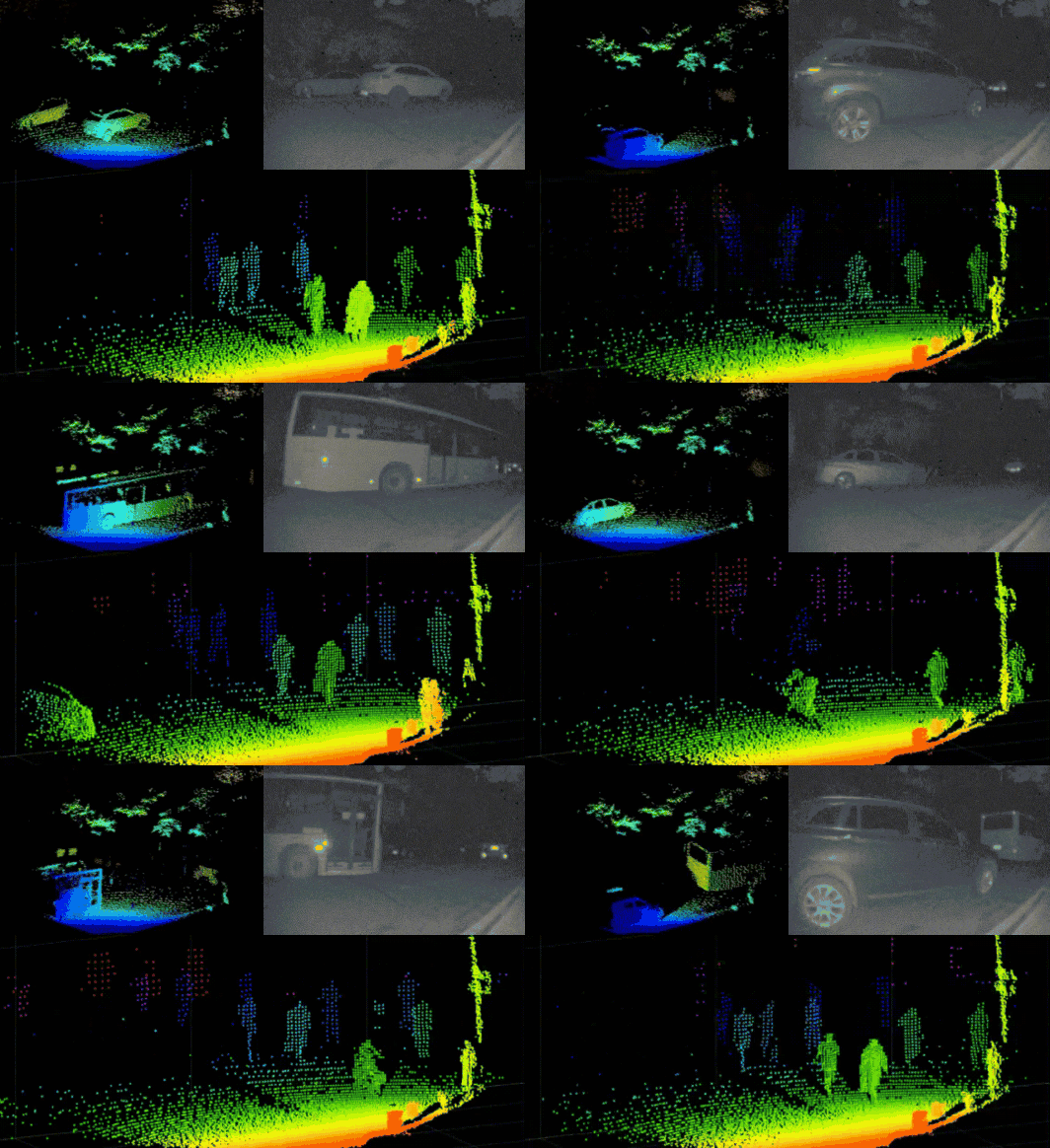
At the same time, Kai Zang has clear views on the future evolution of automotive LiDAR.
First, the endgame for LiDAR is becoming camera-like. In his view, the most mature data systems, algorithm frameworks, and development ecosystems in today's intelligent driving field are almost entirely built around cameras. When vehicles are equipped with both cameras and LiDAR, the two sensor systems often produce two different data sets, requiring additional fusion and calibration. "If future LiDAR can output high-density, regularized array data like cameras, it can naturally integrate into existing algorithm systems."
Second, "this is not just a technical issue, but also a market issue." Today, global annual shipments of camera chips are measured in billions, while LiDAR remains in the millions market. "Only by making LiDAR like cameras can we achieve hundred-million-unit annual shipments."
The key to achieving this goal is complete solid-state transformation of automotive sensors. Kai Zang predicts that whether for front main radars or surround perception radars, all will gradually move away from mechanical scanning and semi-solid-state architectures toward highly integrated array solutions. "The human eye itself is an array perception system, not relying on scanning to acquire information. The perception mechanisms formed through long-term evolution in nature are themselves the best reference answers."
Based on this judgment, Kai Zang points out that future automotive LiDAR will be integrated into a single array chip, with resolution potentially advancing from millions of pixels to tens of millions of pixels, while simultaneously possessing both LiDAR ranging and camera imaging dual functions.
In August 2023, Adaps Photonics successfully launched the 440,000-pixel large-array pure solid-state LiDAR SPAD chip ADS6311. As the world's first 440,000-pixel dToF array chip, the ADS6311 employs a highly integrated pure solid-state architecture, achieving further chipization and scaling of LiDAR's core perception capabilities. In key metrics including precision, resolution, and integration, this product reaches industry-leading levels.
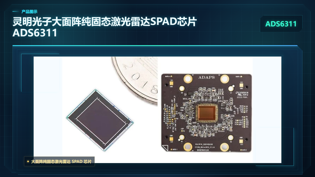
In 2025, the ADS6311 successfully passed AEC-Q102 automotive-grade reliability certification. As one of the first representative products in China to achieve mass production of SPAD array chips and complete automotive-grade verification, the ADS6311 is regarded as an important milestone for pure solid-state LiDAR moving toward large-scale application.
Kai Zang further noted that compared to current semi-solid-state LiDAR solutions, this type of large-array chip offers significant cost advantages; more importantly, it enables natural fusion of LiDAR and camera data at the chip level, eliminating algorithmic ambiguities in temporal and spatial dimensions. The massive data and mature algorithms accumulated across consumer electronics, automotive, robotics, and other industries can all be reused — "from an algorithm perspective, it's also the most streamlined and elegant technical implementation path."

As Adaps Photonics' products continued reaching the market, Kai Zang and his team clearly recognized that SPAD is not technology exclusive to any single industry, but rather an underlying photonic technology with broad extensibility. Whether for intelligent vehicles, robotics, drones, or future data centers and AI infrastructure, the essence always comes down to "optical signal acquisition, transmission, and processing."
Therefore, Adaps Photonics has consistently organized around three core capabilities: optoelectronic conversion, high-speed interfaces, and system-level integration, gradually forming three product directions:
First, LiDAR receiver chips, targeting AI perception scenarios including intelligent vehicles, drones, robotics, and mobile devices, providing machines with precise 3D spatial perception capabilities;
Second, imaging chips, including SPAD image sensors and single-photon 3D cameras, targeting low-light vision, high-dynamic-range imaging, industrial inspection, and special environment perception needs, further expanding the boundaries of machine vision;
Third, optical communications and optical interconnect chips, targeting AI computing infrastructure, supporting the development of future data centers and intelligent computing systems through higher bandwidth and lower power consumption data transmission capabilities.
Around this product layout, Adaps Photonics' technology has gradually been applied across multiple frontier domains including autonomous driving, drones and mobile devices, embodied intelligence robotics, optical communications, and 3D modeling.
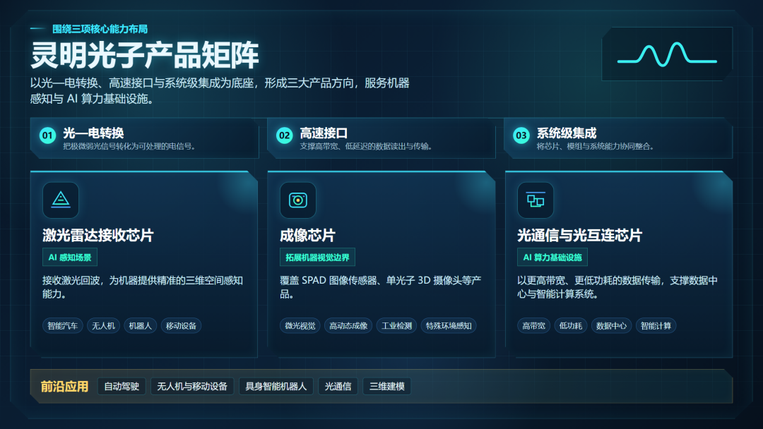
Behind these seemingly diverse scenarios lies the same industrial logic. "Essentially, we've been solving the same problem of how machines acquire information, transmit information, and process information." From LiDAR to image sensors to optical communications, each product extension at Adaps Photonics is not simple business expansion, but natural overflow of the same technology platform across different industry cycles.
This cross-industry extensibility has also become a source of continuous innovation for the company. Rather than searching for markets around a single product, Adaps Photonics focuses on new technology directions that could become industrial infrastructure in 5 to 10 years, and completes early layout. "When new technology cycles arrive, we hope to be among the first enterprises driving advanced technology to scalable implementation," Kai Zang said.

In 2026, Kai Zang and his team began moving into the optical communications field. "This isn't simply crossing boundaries, but a natural extension of platform capabilities. If LiDAR solves how machines perceive the world, then optical communications solves how AI efficiently processes the world."
In Kai Zang's view, the development of the AI era has always revolved around three core elements: data, computing power, and energy.
Over the past few years, Adaps Photonics' main work has concentrated on the data side — using advanced photonic technologies like SPAD to create more affordable, more pervasive sensors, helping systems like autonomous driving, robotics, and drones more accurately acquire and understand real-world information.
As large models and AI infrastructure rapidly developed, the team began turning its attention to another critical capability: computing power. "We've been thinking about whether Adaps Photonics can use our accumulated technical capabilities to solve new bottleneck problems in the AI era."
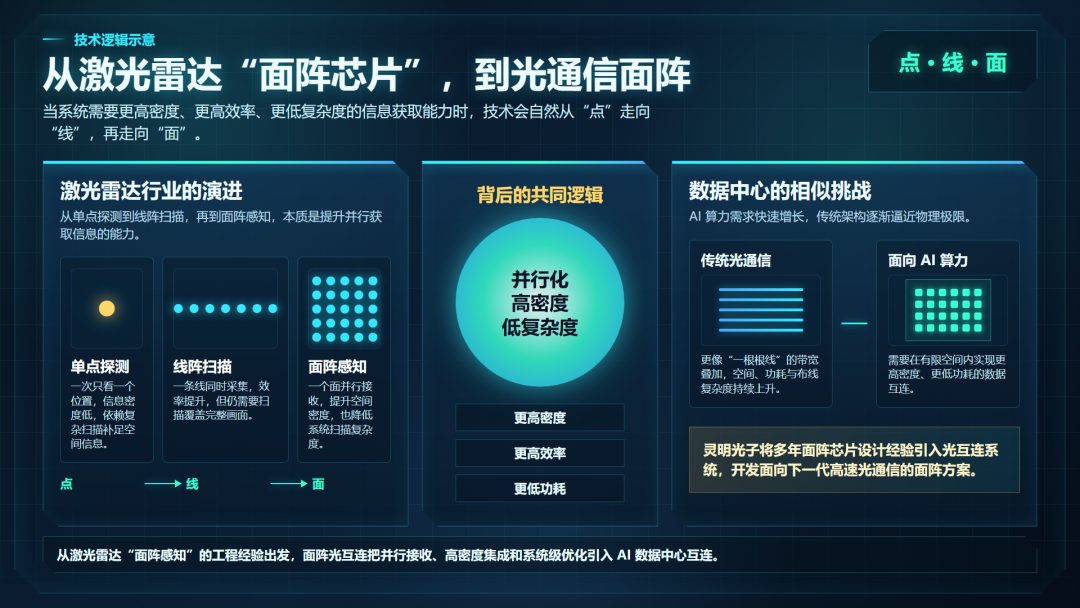
Kai Zang analyzed that the challenges facing data centers today are quite similar to what the LiDAR industry encountered a few years ago — rapidly growing demand, but underlying architectures gradually approaching physical limits. "Assume a single optical fiber carries 100G transmission bandwidth, 8 fibers only achieve 800G, 16 fibers make 1.6T... and so on. Yet physical space around GPUs is limited, and traditional fiber arrangement density has hit a ceiling."
Looking back at LiDAR industry evolution, it progressed from single-point detection to linear array scanning, then to array perception. The logic behind this is simple: when systems need higher density, higher efficiency, and lower complexity information acquisition capabilities, technology naturally evolves from "point" to "line" to "array."
"Optical communications is undergoing similar changes." Traditional optical communications is more like bandwidth stacking of "individual lines," while future AI computing systems need higher density, lower power consumption data interconnection within limited space. For this reason, Adaps Photonics is introducing years of accumulated array chip design experience into optical interconnect systems, developing array solutions for next-generation high-speed optical communications.
Adaps Photonics independently developed an array solution adapted to high-speed optical interconnect systems. On a 20×20 pixel array, it can integrate and arrange 400 optoelectronic channels, with single-area total bandwidth reaching 40T, structurally breaking through spatial and bandwidth bottlenecks in optical interconnection. This technical solution targets achieving 25.6Tbps/mm², potentially providing key device support for new-generation parallel optical interconnect systems. Notably, this solution also possesses extreme low-power advantages. "Today, 70% of data center energy consumption goes to electrical or optical communications. Our solution can effectively reduce energy consumption, aligning with green computing power development trends."
Currently, Adaps Photonics has completed optical communications product prototype construction and will continue iterative optimization. In 2026, the company will launch its optical communications product push, striving for product market launch in 2027 and scaled mass production by 2028.

Looking back on his entrepreneurial journey, Kai Zang believes what has truly mattered is continuously identifying underlying technologies that can transcend industry cycles and continuously spawn new applications. This gives Adaps Photonics confidence to become "the photonic cornerstone of the AI world."
Kai Zang often recommends the book Crossing the Chasm internally. "Getting frontier technology from 0 to 1 is rarely accomplished by a single company alone." It requires early customers, industry partners, and upstream-downstream ecosystems to participate together. It requires people willing to invest in real scenarios when technology is not yet fully mature and commercial returns remain unclear, participating in validation, iteration, and co-creation. "For Adaps Photonics, these partners willing to explore together have been important forces in getting the company to where it is today."
Looking to the future, Adaps Photonics hopes to continue walking alongside more industry partners, continuously crossing the chasm between technology R&D and market application in the evolution of AI perception, AI computing power, and photonic infrastructure, empowering the AI world with hardcore photonic chip capabilities.