MaKe | MaHui Member Suzhou Xihang Semiconductor Technology Co., Ltd. Releases China's First 40nm Bright-Field Nano-Pattern Wafer Defect Inspection Equipment

This marks a new breakthrough for China's domestic high-end semiconductor testing equipment.

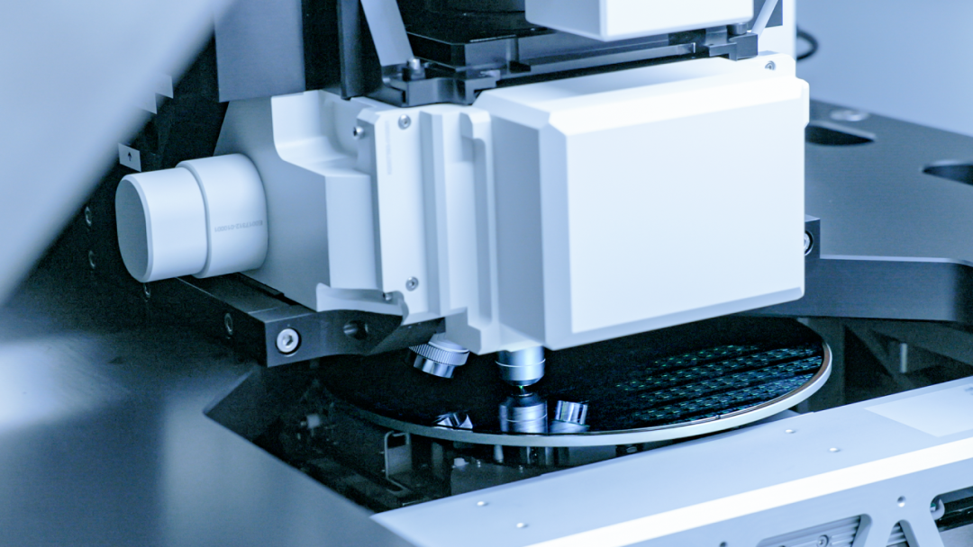
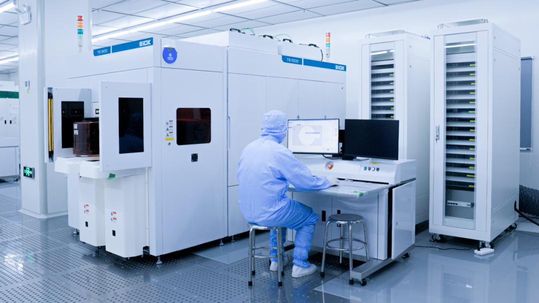
Recently, MaHui member Suzhou Xihang Semiconductor Technology Co., Ltd. (hereinafter referred to as "Xihang Semiconductor") announced that its bright-field nano-pattern wafer defect inspection equipment TB1500, targeting the 40nm technology node, has completed in-factory verification — marking a new breakthrough for domestic high-end semiconductor inspection equipment.
This milestone comes less than a year after Xihang Semiconductor formally delivered the TB1000 in August last year, a wide-band bright-field defect inspection system for 12-inch wafers at the 65–90nm node.
Xihang Semiconductor's core team brings together top talent from leading upstream and downstream players at home and abroad. Leveraging cutting-edge artificial intelligence and ultra-high-precision optomechatronics technology, the company advances semiconductor process improvement and yield enhancement, with the goal of becoming a world-leading semiconductor inspection equipment company. Source Code Capital led Xihang Semiconductor's Series A round.
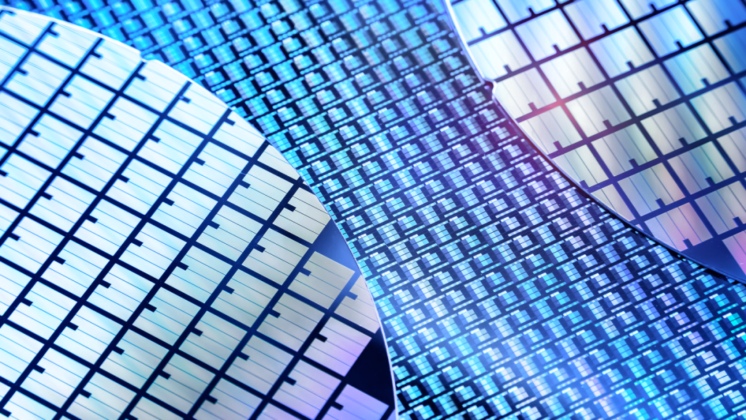
From a full wafer to individual chips, beyond the well-known lithography machines, a series of essential production equipment is required: diffusion furnaces, etchers, ion implanters, thin-film deposition equipment, chemical mechanical polishing machines, and cleaning equipment, among others.
Defect inspection equipment serves as an indispensable tool throughout the chip production process, ensuring chip quality, reducing production costs, and driving process iteration. As process nodes continue to advance and chip manufacturing costs climb, the importance of inspection equipment grows ever greater. Among these, bright-field defect inspection systems — offering higher inspection precision and broader defect type coverage — have become particularly sought-after in the industry.
Founded in November 2021, Xihang Semiconductor represents a new generation of domestic semiconductor equipment vendors. The company has assembled top talent from leading international and domestic semiconductor equipment firms, foundries, publicly listed companies, and research institutions. Focused on the R&D, production, and sales of high-end wafer defect inspection equipment and components, it is working to fill the gap in domestic defect inspection equipment. Backed by an exceptional technical team and advanced technological capabilities, Xihang Semiconductor has gradually broken the monopoly held by foreign players such as KLA over the defect inspection market, injecting fresh momentum into China's semiconductor industry.
The TB1500 is Xihang Semiconductor's latest R&D achievement. All core critical components are fully self-developed and controllable, and the system employs advanced signal processing algorithms to effectively improve signal-to-noise ratio and detection sensitivity. To meet the demands of the 40nm process node, the TB1500 enhances light source brightness and sensitivity while expanding objective lens field of view and speed, enabling the capture of smaller defect sizes.
As artificial intelligence, big data, and other technologies converge and evolve, semiconductor inspection equipment will advance toward greater precision, higher efficiency, and deeper intelligence. Going forward, Xihang Semiconductor will continue to drive technology and product upgrades through its innovation and strategic positioning, striving to become a top-tier semiconductor metrology and inspection company and contributing to breakthroughs in the domestic semiconductor sector.
The company also reports that development of the TB2000, targeting the 28nm node, is progressing smoothly. All core components have been completed, with a prototype scheduled for release by the end of 2024.