4,000 Exhibitors, 190,000 Visitors: Four Shifts in the Optoelectronics Industry | Yunqi Partners x CIOE 2026

AI Infrastructure Emerges as the Defining Theme at This Year's CIOE (China International Optoelectronic Exposition)
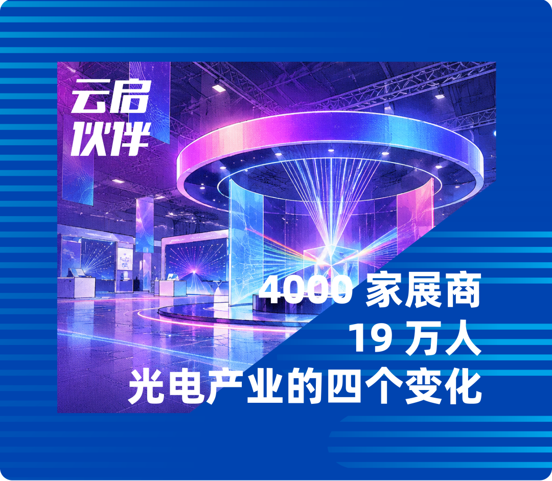
Every September, Shenzhen offers an important window into how the optoelectronics industry is changing.
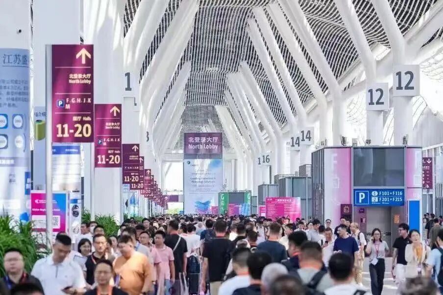
From September 9 to 11, the 27th China International Optoelectronic Exposition (CIOE 2026) was held at the Shenzhen World Exhibition & Convention Center. Official figures put the exhibition area at 260,000 square meters with more than 4,000 participating companies; over three days, attendance reached 189,755, up 32% year over year. After walking the halls for three days, one immediate impression stood out: this year's show shifted its center of gravity from "display" toward "AI infrastructure."
The halls housing optical communications and advanced packaging were the most crowded, and 1.6T, 3.2T, CPO, NPO, and OCS became keywords no forum could avoid.
Yunqi Capital has been investing in optoelectronics and semiconductors for years. This time, three of our early-stage portfolio companies — Nuo Shi Technology, Innovative Semiconductor Substrate Technology Co., Ltd., and Plexin Intelligent — came to the show with their latest progress. In this edition of "Yunqi Partners," we've pulled together the industry shifts we observed at this year's expo along with updates from these three companies, to share with you.

Yunqi's Observations
One noticeable change in the exhibition halls this year: conversations got a lot more concrete. In the past, booth-side conversations usually started with specs: how many PPI, how many nits, what level of precision. This year, the questions asked over and over were about delivery timelines, monthly capacity, and yield. Especially in the optical communications and advanced packaging zones, much of the discussion had moved from "can the product be made" to "when can it be delivered reliably."
Behind this are several industry shifts now underway.
First, competition is increasingly about mass production and delivery capability.
Specs still matter, but for segments that have entered volume ramp-up, customer concerns have clearly moved downstream: when will the production line come online, what's the monthly capacity, can yield hold steady. Some leading manufacturers already have order books stretching into next year, and are starting to discuss demand even further out. Beyond technical capability, manufacturing and delivery are becoming a new dimension of competition.
Second, new optical interconnect architectures like NPO and OCS are moving from roadmaps to engineering validation.
The cross-vendor NPO interoperability demo was one of the more representative developments at this year's show; a number of domestic vendors also brought complete OCS system solutions to the floor. More notable than any single component spec is that the supply chain has begun forming more complete solutions around networking, compatibility, devices, and packaging.
Third, the consumer side is still relatively slow, but costs are shifting.
The AR zone remained lively, and product form factors are getting closer to ordinary glasses. But judging from the show floor, consumer demand hasn't ramped at anywhere near the same intensity. The more certain change is upstream: costs in optical waveguides, nanoimprinting, and related segments continue to fall, leaving room for consumer-grade products to push prices lower.
Fourth, device and equipment makers are entering the supply chain earlier.
In the past, many equipment companies mainly came in at the mass-production stage. This time, it's clear they're participating much earlier — in prototyping, validation, and solution design. Plexin's Fluxless TCB equipment, for example, was already part of the solution at the OCS prototyping and validation stage. As optical modules, OCS, and other systems demand ever higher precision, yield, and consistency, the importance of core devices, packaging, and equipment in the overall solution rises accordingly.
Three Days, 190,000 Visitors:
AI Infrastructure Became the Clearest Through-Line of This Year's CIOE
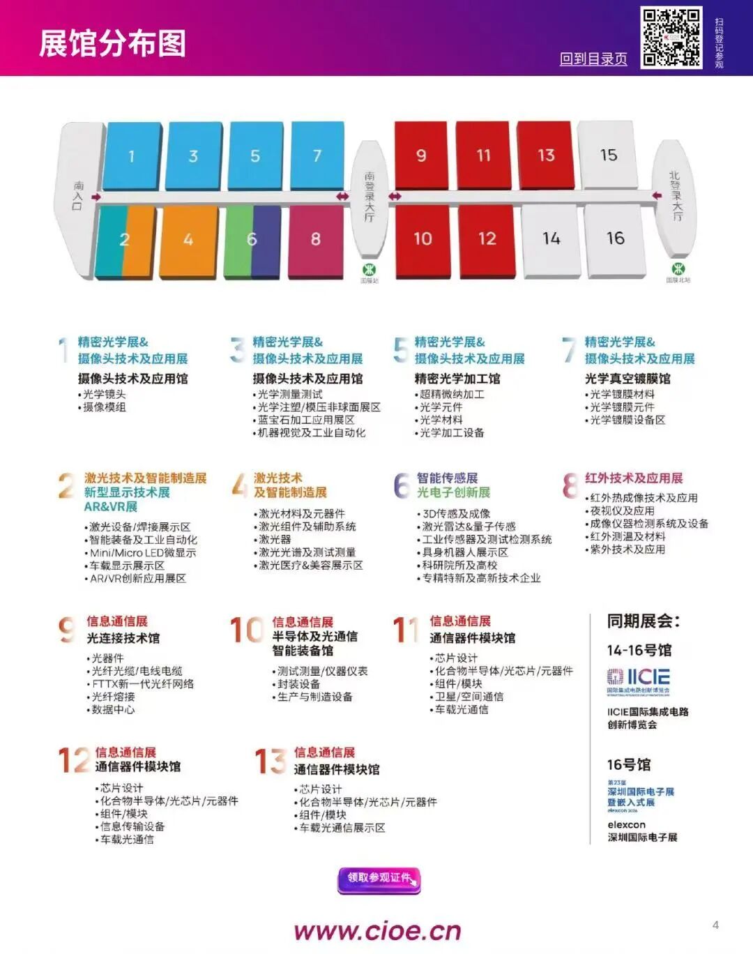
CIOE runs once a year and is one of the few occasions where the global optoelectronics supply chain gathers "full-chain, same venue": from materials, chips, and devices to equipment, modules, and end products, with eight themed exhibitions concentrated in a single exhibition complex. This year it also absorbed the International IC Innovation Expo (IICIE) and the Shenzhen International Electronics Fair (elexcon); combined, the three shows covered 320,000 square meters. Optoelectronics, semiconductors, and electronics have become increasingly hard to view in isolation.
The hall layout itself reflects the industry's current main threads:
- Hall 2 — the New Display Technology Expo linked with the AR&VR Expo, with Micro-LED, silicon-based OLED, optical waveguides, and nanoimprinting concentrated in this area;
- Halls 9–13 — information and communications, covering 1.6T/3.2T optical modules, CPO/NPO, silicon photonics chips, optical engines, and advanced packaging and test equipment;
- Hall 6 — intelligent sensing and LiDAR;
- Hall 10 — semiconductor and optical communications intelligent equipment.
Having attended several editions, the most obvious difference this year is where the industry's attention has landed.
In the past, the hottest part of CIOE was usually "display" — whose screen was brighter, smaller, denser in pixels. This year, the crowds converged on optical communications. AI compute demand has pushed optical interconnects to the front of the industry stage, and 1.6T and 3.2T, CPO and NPO, optical engines and silicon photonics chips became unavoidable topics at nearly every technical forum.
According to public reports, multiple companies on-site spoke of "shortages," "out of stock," and "insufficient capacity," with some high-speed optical chip makers' order books already extending to 2027 or beyond.
And in the new display halls, the focus of discussion also changed: from simply comparing specs toward production lines, yields, and delivery timelines.
Four Changes Worth Remembering
Change One:
NPO and OCS moved from roadmaps onto the show floor On the NPO side, virtually every optical communications vendor worth naming brought a solution, with multiple 3.2T, 6.4T, and 7.2T modules debuting together.
Even more notable than any single product was a cross-vendor demonstration during the show: IPEC, together with multiple member companies, ran a 51.2T NPO switch interoperability test — the switch itself from Huawei, the optical engine from HiSilicon, connecting on the other end to pluggable switches from Meituan and Kuaishou. Measured link latency dropped by an order of magnitude, and total system power consumption fell by more than 20%.
For a new architecture, being able to interoperate with existing equipment means customers don't need to replace their entire network at once — the industrialization significance is often more direct than any single metric. According to Zhongji Innolight's estimates in investor communications, key customers will begin volume procurement of NPO products starting in the second half of 2027.
The shift in OCS (optical circuit switching) was equally visible.
This technology was previously used mainly by overseas cloud providers inside their data centers, with little public discussion in China. This time, companies including Accelink, Bopu Semiconductor, Taclink, Luster LightTech, and Guangdong Sanshiyuan Technology all brought complete system solutions based on different technical paths, and Accelink's 320×320 system ran live at its booth.
Market-side signals are also accumulating: Google is a relatively mature user of this approach; domestically, Huawei's Ascend 950 supernode already uses OCS for inter-rack connectivity; and in early September, Spanish silicon photonics company iPronics closed a $125 million Series B round with NVIDIA participating.
Change Two:
Micro-LED moved from "in development" to "production lines about to go live" In past years, conversations about full-color Micro-LED at booths mostly revolved around "in development" and "in validation." This year, more and more manufacturers started giving concrete production-line timelines.
One long-standing difficulty is red light.
Full-color Micro-LED requires red, green, and blue chips. Blue and green are relatively mature, while red — because it uses a different material system — has long been one of the harder problems in industrializing full-color Micro-LED.
This time, some vendors offered fairly clear progress on-site: Qiushui Semiconductor exhibited a mass-production-grade 8-inch red Micro-LED module, with a supporting 8-inch hybrid bonding line scheduled to come online this October; Sitan Technology's green module reached a peak brightness of 3 million nits and has entered volume delivery; Saphlux's 6-inch silicon-based Micro-LED line has also achieved mass production.
Another change worth noting is how things were displayed.
This year, booths no longer showed just a bare chip. Companies like Raysolve and Hongshi Intelligence began partnering with optical waveguide firms, combining display chips, optical engines, and waveguides of different technical routes to demonstrate complete-device display effects directly.
Moving from supplying a single component to participating earlier in defining complete-device solutions is itself a signal of increasing industrialization.
Change Three:
Optical waveguide costs keep falling
The price band for consumer-grade AR is starting to loosen Optical waveguides are among the most expensive components in AR glasses. Some cost shifts in this segment this year are worth watching.
Goertek Optical exhibited nanoimprinted full-color optical waveguide lenses — 0.5mm thick, 3.2g in weight, with grating-area transmittance above 94% — looking close to ordinary glasses.
Guangna Siwei went further, directly displaying a batch of commercially available AR glasses built on its own waveguides. Its nanoimprinted single-panel full-color solution has brought manufacturing costs down to one-third of mainstream etching-based solutions, or even lower.
The cost decline largely comes from changes in process routes.
Over the past few years, nanoimprinting has gradually moved from an alternative approach into larger-scale industrial application. Tianren Micro-Nano's nanoimprint equipment can now replicate structures with better than 10nm precision on 200/300mm substrates; Pulin Technology delivered an 8-inch wafer-level nanoimprint lithography machine this year, enabling wafer-scale production of photonic chips while bypassing the traditional DUV lithography route, at roughly one-tenth the manufacturing cost of DUV solutions.
For consumer-grade AR to truly reach mass markets, product form factors, content ecosystems, and user demand still need to mature together. But at least on the manufacturing end, costs continue to move down.
Change Four:
Speeds keep climbing
The importance of advanced packaging and bonding rises further Hall 10 was one of the areas most worth lingering in at this year's show.
As optical module speeds move from 400G to 800G, 1.6T, and even 3.2T, how chips and fibers are connected, whether performance holds after connection, and how consistent things are in volume production all directly affect final yield and cost.
As a result, "bonding" and "die attach" — two steps that used to hide deep inside production lines — were pushed to the front of the booths.
The situation with OCS is similar.
Beyond complete-system vendors, companies including T&S Communications, Tengjing Technology, Focuslight, and Fiberhome's optical device peers brought products like MEMS collimator arrays, microlens arrays, and optical circulators. These components aren't eye-catching, but according to cost structures shared on-site, core devices plus precision packaging account for the bulk of total OCS system cost.
When the same process step gets mentioned repeatedly by different vendors, it also signals that advanced packaging and bonding are becoming an unavoidable link in the industry's scale-up.
Three Portfolio Companies On-Site

Nuo Shi Technology | Getting the Chip Itself Right
📍 Hall 2 · 2C126
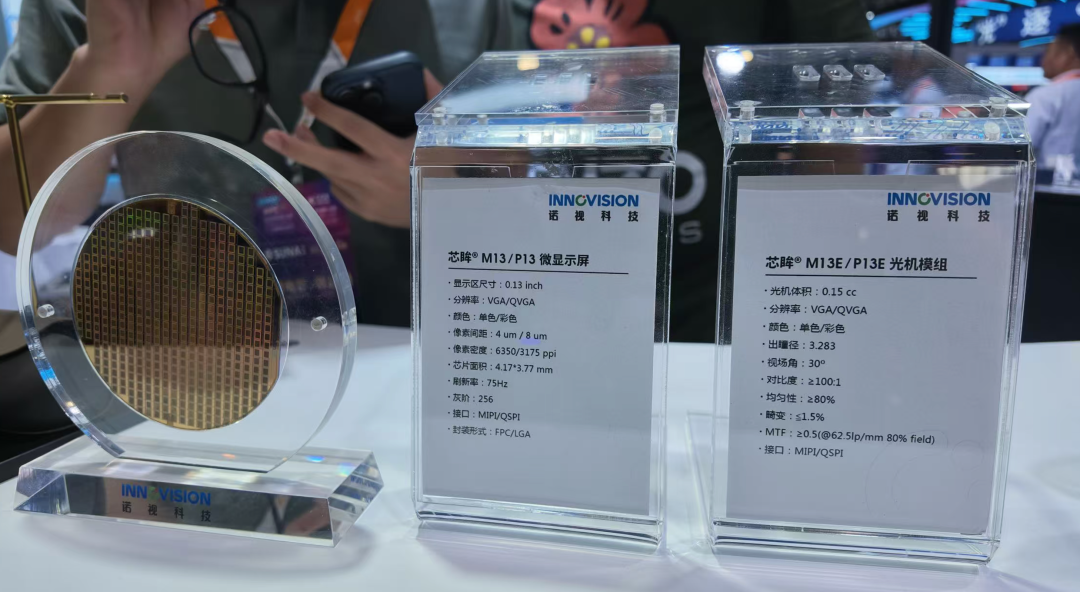
Nuo Shi exhibited four products in its Xinmou® series this time: M06, M06E, M13, and M13E, covering microdisplay chips and supporting optical engine modules. The most watched was the Xinmou® M06: 2.5μm pixel size and roughly 10,000 PPI pixel density. According to the company, this is currently the world's smallest mass-production-grade silicon-based microdisplay product, having completed end-device glasses validation and entered volume delivery. The Thunderbird iO uses the M06, with the device maker then completing integration of the AR-specific optical engine.
Beyond that, Nuo Shi also exhibited the Xinmou® M13 this year, along with the red-green dual-color P13E optical engine module.
The Xinmou® P13, released this June, takes a "single-chip multi-color" route, using one chip to deliver two or more colors, targeting the limitations of monochrome displays in information hierarchy and visibility in complex scenarios. Unlike the mainstream "three-color light combination" approach, it attempts to solve multi-color display directly at the chip-structure level.
Nuo Shi has consistently focused on chip-level consistency, yield, and scaled cost. Technically, it uses its proprietary WLVSP® (wafer-level vertically stacked pixel, or VSP) route, fusing Micro-LED processes with integrated circuit stacking processes on silicon substrates.
The company's production footprint is also fairly complete: headquartered in Suzhou, with a chip production line in Huzhou and a packaging line in Zhuhai, forming a "one headquarters, multiple nodes" structure. It operates an IDM model, laying out the full chain from patent portfolio and product design to R&D, manufacturing, and packaging and testing.
For a microdisplay chip company, bringing packaging and testing in-house means stronger control over yield, cost, and delivery cadence.
This year the company also advanced its material-system choices on red light, adopting a gallium arsenide-based route and achieving 8-inch red epitaxy. If the follow-on processes prove out, it would directly affect scaled costs.
Currently, the company's product strategy is "chip-display integration, display-illumination fusion," with product lines covering AR/VR, HUD, micro-projection, digital automotive lighting, optical communications, and other scenarios.
Innovative Semiconductor Substrate Technology Co., Ltd. | Turning "Bonding" Into a Complete Solution
📍 Hall 10 · 10A21
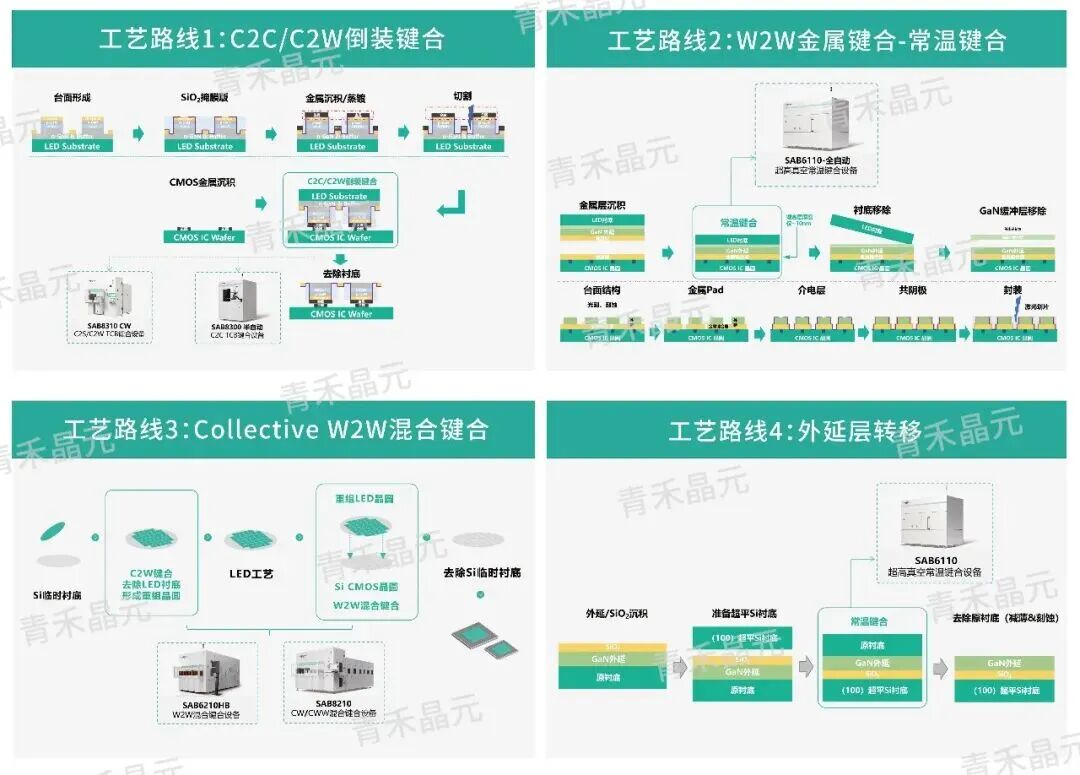
This time, Qinghe (Innovative Semiconductor Substrate Technology) showcased three major bonding solutions built around different application scenarios:
- Silicon photonics heterogeneous integration: addressing pain points like film-thickness uniformity, lattice and thermal mismatch during bonding, and optical heat-dissipation losses, offering a full-process solution combining super-atomic-beam film-thickness trimming (TRIM) with C2W/W2W heterogeneous bonding;
- 2.5D/3D advanced packaging: targeting the precision, yield, and efficiency challenges of hybrid bonding, plus flux residue issues in TCB bonding of large chips, offering a combined solution of hybrid bonding, Fluxless TCB bonding, temporary bonding, and super-atomic-beam surface treatment;
- Micro-LED: addressing utilization losses from wafer-size mismatch and bonding stress from thermal-expansion-coefficient mismatch, offering multiple paths including flip-chip bonding, thermocompression bonding, and room-temperature bonding, covering volume production needs in pixel automotive lighting, AR displays, optical communications, and more.
The company positions itself with a dual-engine model of "equipment manufacturing + precision process services," with a product matrix spanning ultra-high-vacuum room-temperature bonding, hydrophilic/hybrid bonding, thermocompression and anodic bonding, temporary bonding and de-bonding, and super-atomic-beam surface treatment.
During the show, group co-founder and deputy general manager Chao Guo also gave a keynote talk titled "Advanced Packaging and Bonding Technology in the Era of AI Compute" at the IICIE "Advanced Packaging and Test Technology" forum.
Moving from standalone equipment to full-line solutions also means equipment companies are participating more deeply in customers' process flows. As equipment capability, process experience, and production validation gradually converge, their value in the supply chain rises accordingly.
Plexin Intelligent | Domestic Equipment for Optical Module Die Attach
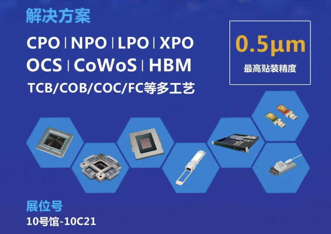
📍 Hall 10 · 10C21
The four machines Plexin exhibited this time correspond to several key process steps in current optical communications manufacturing:
| Equipment | Positioning | Key Capabilities |
|---|---|---|
| Loong | Fluxless TCB thermocompression bonder | ±0.5μm placement accuracy, supports formic-acid-reduction fluxless TCB process, for CPO / NPO / OCS / CoWoS packaging |
| EU406 | Inline thermocompression eutectic bonder | ±1.5μm placement accuracy, three nozzles, dual left-right wafer stages, dual eutectic stages, for COC eutectic die attach of optical modules and lasers |
| Light 2200 | Inline ultra-high-precision die bonder | ±3μm placement accuracy, supports simultaneous multi-chip attach, one-stop die attach for 800G / 1.6T optical modules |
| FAB120 | Fiber array attach machine | ±20μm placement accuracy, automatic plasma cleaning, FA optical-path calibration, FA dimensional measurement, UV curing and closed-loop force control, replacing at least 10 manual operators |
Two developments deserve separate attention.
First, the automation of fiber array (FA) attach.
FA attach is one of the more difficult steps in optical module manufacturing, and one that has relied heavily on manual labor: a ground and polished FA assembly must be aligned to the photonic chip at micron-level precision, then permanently fixed. Precision, force control, adhesive volume, and stress management are all interrelated.
In the past, this step depended heavily on manual work, limiting both efficiency and consistency. Plexin's FAB120/FAB150, launched this year, automate exactly this step.
Second, OCS.
In May this year, Plexin's Fluxless TCB machine Loong worked with a leading overseas OCS developer to complete prototyping validation of the world's first OCS based on silicon photonics CMOS technology.
OCS (optical circuit switching) is a new direction on the data center networking side, replacing part of electrical switching with optical path switching to reduce power consumption and cost. Most related solutions are currently still in the validation stage.
Looking at the company's capability base, Plexin has long built an underlying technology platform: motion controllers, servo drives, linear motors, and machine vision are all developed in-house, extending upward into semiconductor packaging equipment. The company now supplies in volume to most of the world's top ten optical module makers, and has been selected as a national-level specialized and sophisticated "Little Giant" enterprise.
One more piece of industry context: the optical module die bonding/eutectic bonding equipment market is expected to grow from RMB 1.66 billion in 2025 to RMB 6.6 billion in 2030, a compound annual growth rate of about 19%; meanwhile, for high-end die bonding/eutectic equipment targeting 400G/800G/1.6T high-speed optical modules, the domestic substitution rate is currently only around 20%.
Demand is growing fast, and room for domestic substitution remains; at the same time, this is a segment with very high requirements for precision, process accumulation, and production validation.
In Closing
As the three-day show wrapped up, the thing most worth remembering may not be any single spec.
Materials are moving toward larger sizes, chips toward smaller pixels, optical waveguide costs keep falling, and equipment is pushing deeper into higher precision and more complex process steps. Every link in the supply chain is moving forward a little.
These changes ultimately converge on two questions: how long until consumer-grade AR truly reaches mass markets, and how fast the next generation of compute infrastructure can land.
CIOE will return to Shenzhen next year.
By then, the plans on this year's show floor still described as "in validation," "coming online," and "ramping capacity" may well have become new production numbers.